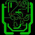
Sorry for the unnecessary lump of track near R13. I t was left there when I was trying to bring the Filter Caps closer the The Outputs!
Bringing the big capacitors in the middle will be very fussy!! Don't you think so??!
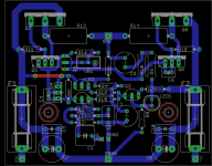
The signal section will sit right in the middle of two big half-winding loops (follow the main current paths!), but many designs follow this basic layout and still works.
For the rest see the image attached (please forgive the kindergarten art...)
The zobel C7/R15 should go in the yellow line.
R4/R5 in the light-blue line, keep traces connected to the bases of Q1/Q2 short.
The purple traces will be the clean "signal ground".
Blue is a jumper that would connect to the power ground.
This could also be a 10 ohm resistor to alleviate possible ground loops.
Or better yet, a wire that connects to the main star ground together with the grounds of the other channels and the grounds of the power supply and speakers.
For the small TO92 transistors, you should have the option in your CAD package to have the pins inline as shown in orange.
These are often easier to route and also allows you to bend the transistor once soldered (e.g. for thermal contact).
You have a lot of space on that board, you could make all the thick traces double of what they are now.
Attachments

Last edited:
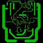
The signal section will sit right in the middle of two big half-winding loops (follow the main current paths!), but many designs follow this basic layout and still works.
For the rest see the image attached (please forgive the kindergarten art...)
The zobel C7/R15 should go in the yellow line.
R4/R5 in the light-blue line, keep traces connected to the bases of Q1/Q2 short.
The purple traces will be the clean "signal ground".
Blue is a jumper that would connect to the power ground.
This could also be a 10 ohm resistor to alleviate possible ground loops.
Or better yet, a wire that connects to the main star ground together with the grounds of the other channels and the grounds of the power supply and speakers.
For the small TO92 transistors, you should have the option in your CAD package to have the pins inline as shown in orange.
These are often easier to route and also allows you to bend the transistor once soldered (e.g. for thermal contact).
You have a lot of space on that board, you could make all the thick traces double of what they are now.
I do have the TO92 with inline pins, but i cannot allign the traces with the pads on the TO92s. I had a doubt, why can't we connect the signal ground to the power ground with the trace? Why a jumper??
I have attached the new layout. Thanks and Regards
Attachments
I had a doubt, why can't we connect the signal ground to the power ground with the trace? Why a jumper??
You can put a trace instead of a jumper.
But using a jumper gives you the flexibility later to replace it with a resistor or to put a separate signal ground wire to the central star ground.
Both measures will improve the amp somewhat.
Note that you miss a main ground connection now...
Try adjusting the editing grid or try the shift/alt/ctrl keys to place a track off the grid to use the inline TO92 package.
Last edited:
You can put a trace instead of a jumper.
But using a jumper gives you the flexibility later to replace it with a resistor or to put a separate signal ground wire to the central star ground.
Both measures will improve the amp somewhat.
Note that you miss a main ground connection now...
Try adjusting the editing grid or try the shift/alt/ctrl keys to place a track off the grid to use the inline TO92 package.
CTRL did the work....thanks!
Is it worth to be the final layout?
Attachments
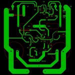
You need a pad on the main ground for the main ground wire, see my sketch of yesterday.
Count them:
Three thick wires coming in from the power supply and star ground: V+, V-, GND.
Two thin wires coming in from signal input connector: Signal, GND.
Possibly a (thin) wire from the star ground to signal GND (or just a jumper as previously discussed).
Count them:
Three thick wires coming in from the power supply and star ground: V+, V-, GND.
Two thin wires coming in from signal input connector: Signal, GND.
Possibly a (thin) wire from the star ground to signal GND (or just a jumper as previously discussed).

Many little irritations, but the basics are there and assuming the layout respects the circuit schematic and your mechanical arrangement, it will work.
The attachment shows a few more suggestions in yellow.
Try to keep tracks 0.04" (1mm) or thicker if you will make the PCB at home.
Make pads as big as possible to allow for holes not drilled center and for eventual component replacement without PCB damage.
The attachment shows a few more suggestions in yellow.
Try to keep tracks 0.04" (1mm) or thicker if you will make the PCB at home.
Make pads as big as possible to allow for holes not drilled center and for eventual component replacement without PCB damage.
Attachments

.....The attachment shows more suggestions.....🙂
Neat and complete, as usual, Mr. Alex. Long awaited...
Thank you!

would agree, very impressive build work and by the look's of things the module's are being linked in bridge mode usage.
alex mm, your pcb designs are works of art 🙂
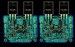
Here's my take on it, from a while ago. Note that I cheated and left the output Zobel off of the board - mine was across the speaker terminals which worked OK. I also added R15 and R17 emitter resistors in the LTP to try this out - but they can be treated as jumpers to stick with the original design. I used a BD140 as the VAS Q4
Here's my take on it, from a while ago. Note that I cheated and left the output Zobel off of the board - mine was across the speaker terminals which worked OK. I also added R15 and R17 emitter resistors in the LTP to try this out - but they can be treated as jumpers to stick with the original design. I used a BD140 as the VAS Q4
Attachments
Many little irritations, but the basics are there and assuming the layout respects the circuit schematic and your mechanical arrangement, it will work.
The attachment shows a few more suggestions in yellow.
Try to keep tracks 0.04" (1mm) or thicker if you will make the PCB at home.
Make pads as big as possible to allow for holes not drilled center and for eventual component replacement without PCB damage.
I'll take ur advice into consideration 🙂
Thank you!
.....The attachment shows more suggestions.....🙂
MR ALEX....!
Your work is really VERY IMPRESSIVE!
Really professional work....!!
Thank your for sharing your layout! 🙂 🙂
Can you tell me what software have you used for making the layout??
Thanks and Regards
Here is another possible combination - since upgraded (5 years of sub duty) with MJL4281A/MJL4302A's.
Thats Clean 🙂
alex mm, your pcb designs are works of art 🙂
Here's my take on it, from a while ago. Note that I cheated and left the output Zobel off of the board - mine was across the speaker terminals which worked OK. I also added R15 and R17 emitter resistors in the LTP to try this out - but they can be treated as jumpers to stick with the original design. I used a BD140 as the VAS Q4
Thanks for sharing your design...Seems like there were loads of Professional Layouts unexposed to this world!
Jaycee,
Nice board layout. Regarding: "I also added R15 and R17 emitter resistors in the LTP . . .", what were the performance results of this change? Adding emitter degeneration in the IPS should improve THD at high frequencies, but might also degrade performance at low frequencies. What was your experience?
Thanks
npdot, at the time I was still learning about power amps, and while i thought it sounded better with 100 ohm emitter degeneration resistors, i don't own any equipment to measure THD or anything like that. It did on the other hand make the pcb layout a bit easier as you can see 🙂
paranoid06, it took me about 6 goes to get that layout, as it was my first PCB design in EAGLE. Expect to have to do it a few times before you get good at it. I don't generally share the design out of respect for Rod - many times I was asked "why don't you just buy Rod's boards?" including once by Rod himself. My answer was I wanted to learn how to do a PCB, which he was happy with. I don't intend to cut into his income though.
paranoid06, it took me about 6 goes to get that layout, as it was my first PCB design in EAGLE. Expect to have to do it a few times before you get good at it. I don't generally share the design out of respect for Rod - many times I was asked "why don't you just buy Rod's boards?" including once by Rod himself. My answer was I wanted to learn how to do a PCB, which he was happy with. I don't intend to cut into his income though.
npdot, at the time I was still learning about power amps, and while i thought it sounded better with 100 ohm emitter degeneration resistors, i don't own any equipment to measure THD or anything like that. It did on the other hand make the pcb layout a bit easier as you can see 🙂
paranoid06, it took me about 6 goes to get that layout, as it was my first PCB design in EAGLE. Expect to have to do it a few times before you get good at it. I don't generally share the design out of respect for Rod - many times I was asked "why don't you just buy Rod's boards?" including once by Rod himself. My answer was I wanted to learn how to do a PCB, which he was happy with. I don't intend to cut into his income though.
Yes, even i don't intend to harm his income....He is a genius and i respect him.
I'm still 15 years old and i don't have enough funds to buy his PCB 🙁
If i buy them then i wont be able to buy the parts then 🙁
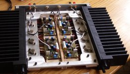
I am an extreme noob.If you read the whole thread, then there have been 5 layouts on expresspcb and 5 layouts on sprint layout. the second lot of the layout was inspired by sakis's layout. I took some idea from the placements of the components on the photo of his completed pcb on his thread.
Regards
npdot, at the time I was still learning about power amps, and while i thought it sounded better with 100 ohm emitter degeneration resistors, i don't own any equipment to measure THD or anything like that. It did on the other hand make the pcb layout a bit easier as you can see 🙂
paranoid06, it took me about 6 goes to get that layout, as it was my first PCB design in EAGLE. Expect to have to do it a few times before you get good at it. I don't generally share the design out of respect for Rod - many times I was asked "why don't you just buy Rod's boards?" including once by Rod himself. My answer was I wanted to learn how to do a PCB, which he was happy with. I don't intend to cut into his income though.
beyond all the above ... for example my choice is to put rail capacitors on board that also cannot be made with rods pcb
- Home
- Amplifiers
- Solid State
- Rod Elliot P3A Layout - Critics