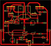
1. Rotate R5 clockwise and get input part closer.
2. Put C+ and C- to the bottom of the PCB, it's necessary to have shorter track as possible.
3. Separate input GND from main GND (get a GND for input from filter caps).
4. You can rotate Q5 180 degrees clockwise, because Q5 doesn't need of any heatsink. U can rotate Q4 also.
5. The + - tracks must be bigger.
BTW is that Sprint Layout file?
Thank you! 🙂
This is an ExpressPCB file...I took the screen shot.
I like the pads of Cadsoft Eagle but don't know to use it 🙁
I don't like the pads of ExpressPCB but I know to use it....!
To make the component pad area bigger, I made rectangles around it!!
Regards
This is an ExpressPCB file...I took the screen shot.
I like the pads of Cadsoft Eagle but don't know to use it 🙁
I don't like the pads of ExpressPCB but I know to use it....!
To make the component pad area bigger, I made rectangles around it!!
Regards
You can try Sprint Layout - got better adjustments and component library.
Great for beginners!
Or search in forum, there's a lot of treads about the legendary P3a.
Great for beginners!
Or search in forum, there's a lot of treads about the legendary P3a.
never post a lay out when its fresh made ... look at it again and again use the advice given ( except the ground issue ) and work on the concept ...
you will find a million other ways to make it better looking and better working
read the forum also .... there is loads of advice on people that tried before you and also there is a lot of advice given to correct the mistakes ..
your pcb will work but its very generic it has a number of things to be corrected
I doubt his pcb will work, has to do at least 10 more revisions.
p.s. Where's the Q6 collector connected to again?
p.s. Where's the Q6 collector connected to again?
Here is the original circuit, for those who are trying to work it all out:
60-80W Power Amplifier
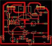
Q9 should line up with Q7 and Q8 because thay all need to be on the same heatsink.
60-80W Power Amplifier
Q9 should line up with Q7 and Q8 because thay all need to be on the same heatsink.
Last edited:
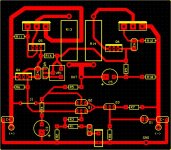
Thank you for your suggestions everybody, I've tried to edit the layout according to Alfonz's suggestions. Hope its better this time!
@sakis - what happens if the layout isn't up to the mark? Will it cause oscillations in the amp??
@kalmara - thank you for letting me know that! That was just something that cannot be avoided! And was out of carelessness.
@ingenius - Is it really necessary to keep them in a line? I was thinking of using U shaped heatsinks used for TO-220s
I've attached the edited layout.
Thanks and Regards
Attachments

Placing Q9 on a heatsink by itself is a recipe for disaster. It provides thermal compensation, therefore it must be on the same heatsink as the drivers (Q7 and Q8). The closer it is to them, the better it will work. This means that your existing layout will have to change drastically, but that is just the way these things work.
Last edited:
Thank you for your suggestions everybody, I've tried to edit the layout according to Alfonz's suggestions. Hope its better this time!
@sakis - what happens if the layout isn't up to the mark? Will it cause oscillations in the amp??
@kalmara - thank you for letting me know that! That was just something that cannot be avoided! And was out of carelessness.
@ingenius - Is it really necessary to keep them in a line? I was thinking of using U shaped heatsinks used for TO-220s
I've attached the edited layout.
Thanks and Regards
Hi paranoid06,
Re your layout - if Q7 and Q8 are vertically mounted on the PCB, you will need to move R13 & R14 away from the top board edge to allow for the heatsink. If you only intend Q7 & Q8 to mount flat on a right-angled bracket, this may not be a problem.
Regards,
currentflow
Placing Q9 on a heatsink by itself is a recipe for disaster. It provides thermal compensation, therefore it must be on the same heatsink as the drivers (Q7 and Q8). The closer it is to them, the better it will work. This means that your existing layout will have to change drastically, but that is just the way these things work.
It's a CFP output stage so thermal linking of the Vbe mult bias transistor is not mandatory
@ingenieus - I guess ur mistaken, Q9 is BC546!
@currentflow - I will be flat mounting them on a right angled aluminium bracket. So no worries! Anyways thanks!
Regards
@currentflow - I will be flat mounting them on a right angled aluminium bracket. So no worries! Anyways thanks!
Regards
It's a CFP output stage so thermal linking of the Vbe mult bias transistor is not mandatory
That applies for the pre-drivers but I'm not so sure about the Vbe multiplier. Douglas Self discusses the difference between thermal compensation for CFP and EF stages at some length in his book. He concludes that CFP has larger bias errors than EF and then describes ways to mount TO225 devices on TO3 or TO3P drivers.
Last edited:
@ingenieus - I guess ur mistaken, Q9 is BC546!
It still has to go on to the heatsink. There are ways to do that. You could glue it on. You could also wrap it in a piece of copper tubing or copper sheet and bolt it down. I'm not sure about what works best. Somebody else might care to comment on this.
That applies for the pre-drivers but I'm not so sure about the Vbe multiplier.
For CFP there is local feedback in the output stage and the Vbe multiplier should be in thermal contact with one or both of the drivers, not OPs, if any.
PS: ESP makes a living from his website, selling PCBs for his projects among other things.
Support him and get the 'reference' boards at the same time!
Last edited:
- Home
- Amplifiers
- Solid State
- Rod Elliot P3A Layout - Critics