Hello Valery
greetings nice front end design can it be tried
warm regards
Andrew
Hi Andrew,
If you wish to try - please go ahead. Let us know how it goes 😉
The topology is rather convenient for a through-hole layout - some others may appreciate your work as well here 😛
Cheers,
Valery
Hello Valery,
You can go even for a simpler VAS: with only one transistor in mirror style.
Keep those compensation capacitors between collectors and ground.
You can go even for a simpler VAS: with only one transistor in mirror style.
Keep those compensation capacitors between collectors and ground.
Hello Valery,
You can go even for a simpler VAS: with only one transistor in mirror style.
Keep those compensation capacitors between collectors and ground.
Hi George, sure - it will work in even simpler configurations.
However the level of VAS linearity (trans-impedance conversion) will somewhat suffer:
- simple mirror with "standard" Hawksford cascode - harmonics level increases roughly 5 times;
- simple mirror with no cascode - harmonics level increases roughly 30 times.
Well, even in the simplest case, performance is not that bad, however - my idea is making VAS as linear as I can, keeping the whole front-end simple enough.
You are always in search for perfection. How do you measure that 0.00006% distortion? Is it worth using 3 transistors instead of one?
Hi Valery,
Looks good!
You can generate very low distortion from very simple compensation schemes. No need for 2 pole comps here.
This current drive VAS would appear to be very linear.
A few ideas...
Have you tried returning R10 and R12 to the junction of R9 and R22. The way you have them configured wastes loop gain. This way you make more efficient use of the available loop gain by "recycling" it (Hope that made sense)
Another change could be to connect R3 to R7? Lose two 0V connections on the PCB.
Could you cascode the LTP transistors off the tails?
Try changing D9 and D16 to LEDs?
It would interesting to try the compensation scheme in my version on this amp.
Paul
You are always in search for perfection.
I am 😀
How do you measure that 0.00006% distortion? Is it worth using 3 transistors instead of one?
This is the simulated value (which is normally close to the measured one on the live prototype). I can physically measure THD values above 0.0001% (-120db) - that's what the external loop-back of my measurement system shows (attached - those are live measurements).
My goal is not just the low THD/IMD - I'm trying to achieve as high open loop linearity as possible. In this case, I don't need too much of NFB to reach low distortion, plus the distortion profile is much better.
Open loop THD of this circuit (no global NFB loop at all) < 0.003% @ 20V RMS ( < 0.008% at 44V RMS) within the whole audio bandwidth (OLG = 82db). This is what I'm looking for. Plus - high speed (wide bandwidth).
Attachments


Hi Valery,
Looks good!
You can generate very low distortion from very simple compensation schemes. No need for 2 pole comps here.
This current drive VAS would appear to be very linear.
A few ideas...
Have you tried returning R10 and R12 to the junction of R9 and R22. The way you have them configured wastes loop gain. This way you make more efficient use of the available loop gain by "recycling" it (Hope that made sense)
Another change could be to connect R3 to R7? Lose two 0V connections on the PCB.
Could you cascode the LTP transistors off the tails?
Try changing D9 and D16 to LEDs?
It would interesting to try the compensation scheme in my version on this amp.
Paul
Hi Paul,
Yes - this approach demonstrates both high open loop linearity and rather wide open loop bandwidth (some 10-20KHz). High accuracy for sure.
The role of R10 and R12 is to slightly shunt the OPS input impedance, decreasing the influence of possible impedance modulation (due to the pre-drivers' base currents change). Well, wasting a little bit of gain, but that's ok as I've got enough of it 😉
R3 to R7 - possible, not really too much difference.
LEDs - possible, but no need - BC546/556 work well at very low Vcb, saving some headroom for the high swings.
Cheers,
Valery
Hi Paul,
Yes - this approach demonstrates both high open loop linearity and rather wide open loop bandwidth (some 10-20KHz). High accuracy for sure.
And by my studies, not picky about output stage. I have a version where performance is the same when using a 3EF BJT or 2 Stage MOSFET output stage.
Also, as you noted, low THD up to clipping.
My version uses about 23dB of feedback flat up to 20Khz. The rest of the loop gain is shunted via the VAS resistor loads. Still gets single digit ppm distortion at 20Khz 2V from clipping in sims. So, yes, this current drive has potential.
The role of R10 and R12 is to slightly shunt the OPS input impedance, decreasing the influence of possible impedance modulation (due to the pre-drivers' base currents change). Well, wasting a little bit of gain, but that's ok as I've got enough of it 😉
Understand. But you get this as well (I think) with the alternative connection. The shunt goes via the feedback shunt resistor. So you still get the shunt effect and you get to linearise the front end some more. And the added bonus of some additional PM/GM as it speeds the front end up as well.
R3 to R7 - possible, not really too much difference.
LEDs - possible, but no need - BC546/556 work well at very low Vcb, saving some headroom for the high swings.
Cheers,
Valery
If you are willing to sacrifice headroom you can create a nice 2 stage clipping effect.
R3 to R7 - Just me and my avoidance of 0V connections where possible. PCB considerations. 😉
Paul
Understand. But you get this as well (I think) with the alternative connection. The shunt goes via the feedback shunt resistor. So you still get the shunt effect and you get to linearise the front end some more. And the added bonus of some additional PM/GM as it speeds the front end up as well.
I will play with this some more time - the way you mention, it's forming a bit of a local FB loop. May give some good effect - agree 🙂
I will play with this some more time - the way you mention, it's forming a bit of a local FB loop. May give some good effect - agree 🙂
Exactly. A local loop. 🙂
Try very low values for these resistors. That's where it gets interesting... THD doesn't increase proportionally while the loop gain is falling. That's what I have found.
If you look at my version I have used the VAS shunt caps to double as MIC caps. Another local loop.
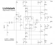
Hi Valery, your Lichtstark is a very interesting design.
I'm wondering if you've seen Mark Johnson's measurements of quasi saturation:
http://www.diyaudio.com/forums/soli...al-npn-no-quasi-saturation-measured-data.html
BC337-40 looks quite good, BC550C is not as good but better than many others.
ZTX851 looks to be the best of the group tested.
Something to consider for the VAS.
What version of SPICE are you using? I don't think that LTSPICE models quasi sat.
Hi Valery, your Lichtstark is a very interesting design.
I'm wondering if you've seen Mark Johnson's measurements of quasi saturation:
http://www.diyaudio.com/forums/soli...al-npn-no-quasi-saturation-measured-data.html
BC337-40 looks quite good, BC550C is not as good but better than many others.
ZTX851 looks to be the best of the group tested.
Something to consider for the VAS.
What version of SPICE are you using? I don't think that LTSPICE models quasi sat.
Hi Pete,
Good point - thank you for reminding me about Mark Johnson's good work.
ZTX851/951 pair looks good for sure - I will try it in the sim and then see what difference the live prototype is going to show.
I'm using Multisim for simulations, using the bc546/556 models provided with the package. Diodes give the Spice models for ZTX851/951 on their web site - I'm going to try to use those.
Cheers,
Valery
...I don't think that LTSPICE models quasi sat.
It does, Multisim too, Valery do you use the quasi-saturation parameters?
Best wishes
David
Last edited:
It does, Multisim too, Valery do you use the quasi-saturation parameters?
Best wishes
David
Hi David,
I'm actually not that versed in the model parameters - can you please look at them. For example, here is one of the models I use (SMD part BC846B):
**********************************************************
*
* BC846B
*
* NXP Semiconductors
*
* General purpose NPN transistor
* IC = 100 mA
* VCEO = 65 V
* hFE = 110 - 450 @ 5V/2mA
*
*
*
* Package: SOT 23
*
* Package Pin 1: Base
* Package Pin 2: Emitter
* Package Pin 3: Collector
*
*
*
* Simulator: Spice 2
*
**********************************************************
*#
.MODEL QBC846B/NXP NPN
+ IS = 1.822E-14
+ NF = 0.9932
+ ISE = 2.894E-16
+ NE = 1.4
+ BF = 324.4
+ IKF = 0.109
+ VAF = 82
+ NR = 0.9931
+ ISC = 9.982E-12
+ NC = 1.763
+ BR = 8.29
+ IKR = 0.09
+ VAR = 17.9
+ RB = 10
+ IRB = 5E-06
+ RBM = 5
+ RE = 0.649
+ RC = 0.7014
+ XTB = 0
+ EG = 1.11
+ XTI = 3
+ CJE = 1.244E-11
+ VJE = 0.7579
+ MJE = 0.3656
+ TF = 4.908E-10
+ XTF = 9.51
+ VTF = 2.927
+ ITF = 0.3131
+ PTF = 0
+ CJC = 3.347E-12
+ VJC = 0.5463
+ MJC = 0.391
+ XCJC = 0.6193
+ TR = 9E-08
+ CJS = 0
+ VJS = 0.75
+ MJS = 0.333
+ FC = 0.979
Here is the model for ZTX851 provided by Diodes on their web site (rather old Zetex model):
*ZETEX ZTX851 Spice Model v1.0 Last Revised 21/1/93
*
.MODEL ZTX851 NPN IS =1.0085E-12 NF =1.0001 BF =240 IKF=5.1 VAF=158
+ ISE=2E-13 NE =1.38 NR =0.9988 BR =110 IKR=5.5 VAR=46
+ ISC=4.6515E-13 NC =1.334 RB =0.025 RE =0.018 RC =0.015
+ CJC=155E-12 MJC=0.4348 VJC=0.6477 CJE=1.05E-9
+ TF =0.79E-9 TR =24E-9
*
*$
*
Thank you,
Valery
I have just checked the voltages for Q7, for example:
Vcb = 600mV
Vce = 1.28V
Those are low enough, but they stay rather constant at all times (this is a part of the current mirror) - fluctuation of Vcb is less than 15mV at the output swing at Q8's collector being 108Vpp.
Vcb = 600mV
Vce = 1.28V
Those are low enough, but they stay rather constant at all times (this is a part of the current mirror) - fluctuation of Vcb is less than 15mV at the output swing at Q8's collector being 108Vpp.
I'm actually not that versed in the model parameters - can you please look at them.
No quasi-saturation parameters in either model.
But I am not yet that versed in the details either, so not sure if it would make much difference in your results anyway.
Those results show a lot of promise, what was the full power, output included 20 kHz distortion?
Best wishes
David
Hi Valery,
in order to minimize DC offset, wouldn't it be preferable to return the U1/U3 bases to ground via a resistor of the same value as the NFB path resistor R22 and to inject offset correction voltage, if still any needed, into the R9/C1 connection?
Best regards!
in order to minimize DC offset, wouldn't it be preferable to return the U1/U3 bases to ground via a resistor of the same value as the NFB path resistor R22 and to inject offset correction voltage, if still any needed, into the R9/C1 connection?
Best regards!
It does, Multisim too, Valery do you use the quasi-saturation parameters?
Best wishes
David
Right I should have said the models that most of us use do not have the parameters.
VBIC models are needed I believe.
I don't know if there is discussion about it in the Yahoo user's group or not.
I just looked up the ZETEX ZTX851 and it is a 5 Amp part with a lot of capacitance.
I'm not that familiar with ZETEX parts so should have looked it up earlier.
Kind of amusing that the ancient 2n4401 and PN2222A look so good.
KSC2690AY looks very good, I like it.
I'm not that familiar with ZETEX parts so should have looked it up earlier.
Kind of amusing that the ancient 2n4401 and PN2222A look so good.
KSC2690AY looks very good, I like it.
Last edited:
- Home
- Amplifiers
- Solid State
- Revisiting some "old" ideas from 1970's - IPS, OPS