Hi friend,
Pehaps you would be int6in reading through the Slewmaster thread and see just how many different IPS sections were happily married to the the 3ef BJT OPS. I would certainly not call it a tough affair. If will make you happy I will gladly hook any of these IPS up to my Slewmaster 5 pair BJT OPS and post some sine and square waves.
Blessings, Terry
Thanks but that thread is somewhat...very long. Could you tell me which has actually been built and tested with a complex load? Thanks. And i don't need more than 50 watts. You know the hardest thing is to fit the diy amp in a proper enclosure. So i don't do that but prefer active speakers. There are restrictions to meet such as heatsink size transformer size etc.
BJT are current multipliers.
No... I don't want to fight for that - I'm a very friendly guy 🙂 But this is only "true" for some simplified calculations. If you look at the accurate BJT model - like Ebers-Moll equation - BJT is a transconductance device, just like a JFET. The independent variable in the Ebers-Moll equation is Vbe. Not base current!
There's simply no little demon in the base, counting electrons moving through the base, and dispensing β times that many electrons into the collector 😉
No it is semiconductor physics. But that is truly academic. There is a standard textbook about this. I don't even know where to find it in my library. But a long time ago i designed very fast logic with bjt, ECL and such. I mean the chips. That makes direct use of the physics of semiconductors.
Hi Guys,
Is there more information about the Non-switching Class A driver stage OPS? I'm trying to get it finished but I can seem to find the schematic.
Thanks, Terry
Is there more information about the Non-switching Class A driver stage OPS? I'm trying to get it finished but I can seem to find the schematic.
Thanks, Terry
Hi Guys,
Is there more information about the Non-switching Class A driver stage OPS? I'm trying to get it finished but I can seem to find the schematic.
Thanks, Terry
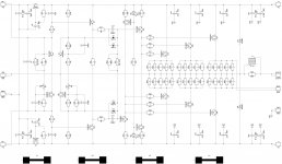
Hi Terry, schematic is in the post #144.
Cheers,
Valery
Hi Valery,
Thanks. Not sure how I missed it. The silk doesn't show the orientation of the TO-126 devices. I need the schematic to make sure they are right.
Blessings, Terry
Thanks. Not sure how I missed it. The silk doesn't show the orientation of the TO-126 devices. I need the schematic to make sure they are right.
Blessings, Terry
Valery ,
can you try to explain how the non switching circuit works... Do you have any device voltage/current plots over the 0 crossing line.. What is the Idle current?.
can you try to explain how the non switching circuit works... Do you have any device voltage/current plots over the 0 crossing line.. What is the Idle current?.
Valery ,
can you try to explain how the non switching circuit works... Do you have any device voltage/current plots over the 0 crossing line.. What is the Idle current?.
Hi Michael,
The principle is very simple yet efficient.
The first Vbe spreader, on the left (Q3, Q4) sets the quiescent current at no signal conditions - as usual.
The second Vbe spreader (Q5, Q6) - sets the minimal bias, making sure the collector current of the inactive shoulder comes close to zero, but never touches it, preventing the output transistors from closing completely.
Then, there is a diode clamp (D1-D4) - that's the mechanism, making this bias limiting happen. It is important to use rather fast devices in both the second spreader and the clamp to ensure smooth operation (no artifacts) at the higher end of the audio bandwidth.
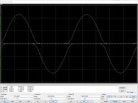
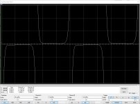
The pictures below show the voltages at the emitter resistors of the output pair, equivalent to the collector current curves (left - full picture, right - close-to-zero area closeup). You can see, it comes close to zero, but never crosses it (in the normal push-pull EF it always does). You can also see, the limiting is rather soft - no sharp corners - which is also good to have.
I have received the PCBs and starting soldering one channel - we'll see it live soon 😎 Although, Terry can do it quicker, as usual 😉
Cheers,
Valery
Attachments
Q3 serves temperature dependent VBE? but Q5 does not? Or both are thermally coupled?
Q3-Q6 are all placed on the main heatsink, under the board, in particular positions.
Attachments

I need to make some time to assemble a set of these boards. It looks like an interesting design to experiment with.
I need to make some time to assemble a set of these boards. It looks like an interesting design to experiment with.
Yep 🙂 I'm soldering mine right now 😉
I'm mid way through building a constant current supply for an anodizing tank. I want to make a bunch of chassis to put all these amps into before I end up buried in them like Terry. 😀
Very interesting!I'm mid way through building a constant current supply for an anodizing tank. I want to make a bunch of chassis to put all these amps into before I end up buried in them like Terry. 😀
I have them ready to mount on a heatsink so I can solder up the under board devices. Clearing up a large heatsink that I can mount them to. Man these things need a lot of real estate.
Q3-Q6 are all placed on the main heatsink, under the board, in particular positions.
Ok that requires some skills. I think "non switching" has no advantage over class AB at higher levels but could have audibly and measurably advantages at low levels. Very few magazines - and DIY - really test at 50mWatt - 150 mwatts. But it is worth.
Hi Valery,
This is probably a bad time for you. I never can keep track of when you are sleeping.
I am ready to test the big OPS but I don't know the procedure for setting the trimmers. If you can please run me through it.
Thanks, Terry
This is probably a bad time for you. I never can keep track of when you are sleeping.
I am ready to test the big OPS but I don't know the procedure for setting the trimmers. If you can please run me through it.
Thanks, Terry
Yes,amplifiers and preamplifiers everywhere.....no chassis no heatsinks......😱You must be knee deep in amplifiers by now too Thimios.
This travel is long,too long and expensive,i believe that i must be stop because of the money.
The good news is that i have friends all over the world,they offer to me a lot of parts.🙂😉
Thank to all of you🙂
Last edited:
Yes,amplifiers and preamplifiers everywhere.....no chassis no heatsinks......😱
This travel is long,too long and expensive,i believe that i must be stop because of the money.
The good news is that i have friends all over the world,they offer to me a lot of parts.🙂😉
Thank to all of you🙂
We see the value of a good tester.
- Home
- Amplifiers
- Solid State
- Revisiting some "old" ideas from 1970's - IPS, OPS