
Hi Marcel
I am waiting for boards and components to make a version of your RTZ FIRDAC.
As PS for this I would very much like to use LIFEPO4 batteries and avoid all LDO´s.
3,3V is no problem as this is the nominal voltage of one LIFEPO4 cell.
5 V is a little trickier , but as I see it in the data sheets of the 5 V logic, all has a max voltage of 7V and the nominal voltage of 2xLIFEPO4 is 6,6V,. Of cause there has to be some monitoring of the voltage , so it is prevented from deliver MORE than 7V, but that is not difficult.
+/- 15 V for the reference and filter section I guess I can use 16,6 V instead from 5x LIFEPO4 cells as the max. voltage for OPA2210 is +/- 20V.
Any comments to this?
Some of the 5 V logic ICs actually have 6.5 V rather than 7 V absolute maximum ratings, for example the Nexperia 74LVC1G74 and the Texas Instruments SN74LVC1G74. In any case, I can think of two disadvantages of using a higher than normal supply voltage.
First, the switching thresholds of the HCT and AHCT ICs used at the inputs will increase, so they may not be TTL compatible anymore. It's probably a non-issue; I don't expect the thresholds to increase so much that they don't understand 3.3 V CMOS levels anymore.
Second, long-term degradation effects such as hot carrier degradation and negative-bias temperature instability will get worse, reducing the lifetime of the CMOS chips that run at 6.6 V instead of 5 V. I have far too little information to predict how much. These effects usually quickly get worse with temperature, so it may be a good idea to ensure that these ICs don't get placed near anything hot.
Marcel.
Another question. Did you ever try the passive filter you made for yor tube dac in the RTZ-FIRDAC?
The driving impedance it was designed for is much higher than the RTZ shift register FIRDAC's output impedance. Nonetheless, you could design a passive filter that works with the RTZ shift register FIRDAC's output impedance. A disadvantage is that it won't work as a virtual ground at any frequency, worsening the data-dependence of the reference current. Whether that matters much, I don't know.
Hi MarcelSome of the 5 V logic ICs actually have 6.5 V rather than 7 V absolute maximum ratings, for example the Nexperia 74LVC1G74 and the Texas Instruments SN74LVC1G74. In any case, I can think of two disadvantages of using a higher than normal supply voltage.
First, the switching thresholds of the HCT and AHCT ICs used at the inputs will increase, so they may not be TTL compatible anymore. It's probably a non-issue; I don't expect the thresholds to increase so much that they don't understand 3.3 V CMOS levels anymore.
Second, long-term degradation effects such as hot carrier degradation and negative-bias temperature instability will get worse, reducing the lifetime of the CMOS chips that run at 6.6 V instead of 5 V. I have far too little information to predict how much. These effects usually quickly get worse with temperature, so it may be a good idea to ensure that these ICs don't get placed near anything hot.
Thanks a lot for all your answers!
I didn´t see at first , that you used the +5V to power the 74LV IC´s I thought you used 3,3V there.
So instead of batteries for the +5V I plan on using two 3000F 2,7V in series with a 5V/5A charger that is active whenever the mute signal or no dsd data is saying , there is no music playing.
The stored energy in 1500f/5V is around 5Wh and as the current consumption in the 5V supply is between 43.8 and 51,8 mA it is using 0.25 W so it will play for a loong time, if my calculations are correct 😁
Koldby
Suppose you want to keep the voltage between 4.5 V and 5.5 V. After charging them to 5.5 V, you can then draw 1500 C of charge from the series-connected supercapacitors. That will take 30 000 seconds at 50 mA, or 8 hours and 20 minutes. If you only charge them to 5 V, 4 hours and 10 minutes. Sounds feasible.
How big are 3 kF supercapacitors? The largest I've ever used were 300 F and looked like rather big PCB-mounted electrolytic capacitors.
How big are 3 kF supercapacitors? The largest I've ever used were 300 F and looked like rather big PCB-mounted electrolytic capacitors.
The state of the art super capacitor is 138 X 60 mm.
chrome-extension://efaidnbmnnnibpcajpcglclefindmkaj/https://www.eaton.com/content/dam/eaton/products/electronic-components/resources/data-sheet/eaton-xl60-supercapacitors-cylindrical-cells-data-sheet.pdf
You can get them at a lower price, but I guess you have to be careful not to buy something that is not what it claims to be.
Eaton is a brand with relatively good reliability and lifetime figures, especially when you look at the typical data in their application notes. They're better in that respect than any other brand I found, actually. Even then, it's important to ensure the supercapacitors don't get hot.
Latest iterations of my 2 RTZ DAC units:
DAC1:

DAC2:

I have gone away from Logitech SB Receiver and Transporter as streamers now and concentrated on piCorePlayers and JLSounds I2SoverUSB as that route is clearly superior. (Plus I get the option to use a PC to drive the JLSounds with HiRes and/or direct DSD)
With the help of Mark's reclocker and my own derivation of a customized subset specifically designed to fit into my available space in the enclosures I now also have external XOs and reclocking of the DSD signals. There are compromises made but it was time to get these projects completed to the point I can put the lids on and move to the next thing before my interest wanes. I was up to version 11 of the reclocking pcb so it was time to admit I'd reached the point of diminishing returns!
DAC1:
DAC2:
I have gone away from Logitech SB Receiver and Transporter as streamers now and concentrated on piCorePlayers and JLSounds I2SoverUSB as that route is clearly superior. (Plus I get the option to use a PC to drive the JLSounds with HiRes and/or direct DSD)
With the help of Mark's reclocker and my own derivation of a customized subset specifically designed to fit into my available space in the enclosures I now also have external XOs and reclocking of the DSD signals. There are compromises made but it was time to get these projects completed to the point I can put the lids on and move to the next thing before my interest wanes. I was up to version 11 of the reclocking pcb so it was time to admit I'd reached the point of diminishing returns!
How to make a balanced DAC? Directly parallel? X2 module? What is the frequency that needs to be blocked in the simulation section
Last edited:
Okay, that's what I've been wanting to ask, but I'm looking forward to the release of your new FPGA and discrete output circuit.
How to make a balanced DAC? Directly parallel? X2 module? What is the frequency that needs to be blocked in the simulation section
It's balanced by design, so I don't understand the question. What do you mean by "the simulation section"?
For anyone who wants to try out my interpretation of @Markw4's XO and re-clocking design I have attached the Schematic, Gerbers and BOM files,
My intention here was to try out external XOs and reclocking for the I2SoverUSB / PCM2DSD but also fit within the size constraints of my already constructed two RTZ DACs. After experimenting with Mark's design and also with his advice and comments I (eventually) arrived at version 11 of the pcb! I am not saying this is as good as Mark's design since I made compromises and went my own way on some component choices to an extent, generally to make the board fit the space I had.
I am positive that more can be done and perhaps I made schoolboy errors so please go easy on me! 🤓
I did have some issues with the switchover between the two XOs and this ultimately seemed to be the result of the clock doubler PLL throwing a fit when changing over due to the fact that initially I was also disabling the unused XO. The XOs are now on constantly. Anyway, the latest version has a few selectable solder pins to accommodate using either 22/24Mhz XOs or 45/49. (or indeed only using one of choice) Plus a site for a 3rd party 317 pin-out reg to experiment with different LDOs.
Attachments
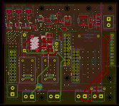
I should probably just make clear. What I just posted is a carrier board for both I2SoverUSB FIO and PCM2DSD. I2SoverUSB is on top and PCM2DSD is slung underneath. Connections to Marcel's DAC are via u.fl leads and the two aux signals DSDon and Mute are via hardwires,
Hi Tony,
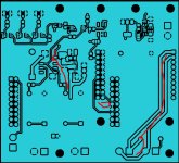
I see some issues with the gerbers you might want to check into. There are some areas of floating copper, which is not good. For instance the top copper layer looks the attached in Kicad Gerber Viewer. Areas marked in red appear to be floating. They should probably be connected by vias to ground (or some other net), or else made into rule areas where fill is not applied.
EDIT: From looking at the pic you posted, it appears there are lot of ground vias. Don't know why they don't appear in the top copper layer of the gerbers. Maybe the gerbers are from an earlier version?
Attachments
Last edited:
Hi Tony,
Looks like some of those vias only show up in the drill file. IOW, the top copper is drilled out after etching to produce vias.
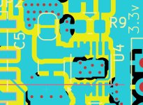
Still, in some areas its pretty hard to check the layout. For instance, in the attacked pic it pretty hard to figure out exactly what is going on with some of the gerber views.
Maybe you could send me the kicad files so I can take a better look?
Best,
Mark
Looks like some of those vias only show up in the drill file. IOW, the top copper is drilled out after etching to produce vias.
Still, in some areas its pretty hard to check the layout. For instance, in the attacked pic it pretty hard to figure out exactly what is going on with some of the gerber views.
Maybe you could send me the kicad files so I can take a better look?
Best,
Mark
Attachments
Last edited:
Hi Mark,
I've sent you the KiCad archive. It is entirely possible I missed some vias during one of the re-versionings. Fatigue sets in after a while!
Thanks for your feedback.
Cheers,
Tony
I've sent you the KiCad archive. It is entirely possible I missed some vias during one of the re-versionings. Fatigue sets in after a while!
Thanks for your feedback.
Cheers,
Tony
Once revised I'm interested if the price isn't too high & if it's compatible with Amanero Combo768?
I've sent you the KiCad archive. It is entirely possible I missed some vias during one of the re-versionings. Fatigue sets in after a while!
Hi Tony,
Sent you a PM regarding some possible issues.
For other folks, maybe good to hold off on this version for the moment.
Cheers,
Mark
I'll be looking at updating to version 12 this weekend to take onboard Mark's review and to split to separate relays for the two XOs. It will necessitate an increase in board size but hopefully I can fit it in within the constraints of the pcb manufacturer's limits to get the best price.
I will grab some more space in the vertical direction (as in the image shown previously) and so will also have the advantage of moving the XOs further away from the PCM2DSD underneath and the other sensitive components, including the LDO.
I should also note that although I did put Mark's name on the pcb that was to acknowledge the advice he's been providing to me as I learn, plus the whole concept was closely derived from his general purpose clock board design. So any blame regarding imperfections in the pcb layout lay squarely with me! 🤣
- Home
- Source & Line
- Digital Line Level
- Return-to-zero shift register FIRDAC