Indeed there is an audible effect in Marcel's RTZ dac depending on output switch decoupling capacitor type. An audible effect there would seem to imply that varying current is being drawn by the switches depending on data, and or there is an imbalance in current draw from both phases of the dac output if loading is unequal. My test with film decoupling caps suggested that more linear caps can help moderate the audible distortion effect (distortion and or correlated-noise that sounds like distortion), but it also showed that different types of caps can have an effect on the 'voicing' of the dac sound. Thus the X5R caps were left in place for the remaining time the dac was available. Putting a 120R metal film resistor in parallel with each bypass cap did seem to result in some improvement in Vref stability, with a corresponding reduction in audible the distortion effect.The waveform of the current drawn from the reference then becomes data-dependent...
In the case of Andrea Mori's DSD dac which was mentioned as an example, each FF output switch has its own local physically small, thus low inductance SMD film decoupling cap (1uf?). IMHO the more linear decoupling design does seem to help locally even out Vref stability despite some possible data dependent variation in current draw resulting from sub-nanosecond timing skew.
Last edited:
Good morning to you ... and Marcel once again many thanks for your feedback. I realize my post was very unusually long - appreciate that you replied to it ;-)
First a brief comment to Mark's post #1921: As part of this investigation into the clock signal I also tried to find a specification for the inter-gate skew on typical logic ICs. And according to a post in TI's EE forum they expect CMOS ICs inter-gate skew to be less than 250 ps although this is not guaranteed.
https://e2e.ti.com/support/logic-gr...en-logic-device-what-is-the-part-to-part-skew
My personal guess (and it is a guess although based on the NB3L553 datasheet specifications) is that IC to IC skew may/might be more than this.
And then a few comments in relation to Marcel's feedback:
It is calculated in the Saturn PCB toolkit crosstalk calculator to my memory using ~1 ns rise time, 5mm coupled length, a 0.2mm trace-to-GND layer distance, and an FR4 board. As far as I understand it includes an underlying GND layer but I don't know if it also considers a top layer GND fill. But if I am not mistaken a top layer GND fill without stitching vias would not make that much of a difference ... ?
Since I was (& have many times been, actually) surprised by the high level of crosstalk that will be experienced in a typical digital circuitry I have checked the SPT values with other calculators on the internet and they are very close. However, my guess is that the calculators do not take into account a top GND fill, nor stitching vias, etc.
Ah, I see 😉 .. That is the reason why you have connected (most) all the GND connections in the layout? BTW, if interesting, Robert Feranec has a video clip on the effect of via stitching here (quite a difference IMHO):
Time 16:03
Hmmm ... when you say transition time do you then mean rise/fall time? I don't think SPT considers driving impedances but would this be necessary to consider? Isn't crosstalk an "instantaneous" phenomenon caused by the local influences of electrostatic & inductive effects ... ? If the driving impedances were to be considered then somehow the distance (time delay) to the driver would also matter, would it not? Just thinking aloud here - not something I know much about.
I also think it will be a very short peak - and as I mentioned essentially all the "clocked" logic ICs I have come across have their timing pins placed immediately adjacent to some other data pin.
As I was thinking about it "No". Sometimes it just is my impression that many of the rules of thumb in digital design originate from the "pure" digital design world, i.e. maybe with a main focus on signal integrity, and thus they may not necessarily we directly applicable to the world of audio. Anyway, I just tried to calculate how much the capacitance of two directly crossing wires is (0.3mm width, 0.2mm spacing, FR4) and it is ~20 fF. Which with a 50 ohm driving impedance, 5V signal and 1ns rise time gives an instantaneous current of 100 uA.
Thank you also for the link to the article. I have briefly looked at it but as I think you know I am not that mathematically "strong". I was more hoping for a "guesstimate" - that one of you might have thought about this already.
Hmmm ... interesting information, sounds very reasonable. So ideally the gates should be clocked at exactly the same time - it makes sense.
Cheers & thanks again for replying, Marcel 😉
Jesper
First a brief comment to Mark's post #1921: As part of this investigation into the clock signal I also tried to find a specification for the inter-gate skew on typical logic ICs. And according to a post in TI's EE forum they expect CMOS ICs inter-gate skew to be less than 250 ps although this is not guaranteed.
https://e2e.ti.com/support/logic-gr...en-logic-device-what-is-the-part-to-part-skew
My personal guess (and it is a guess although based on the NB3L553 datasheet specifications) is that IC to IC skew may/might be more than this.
And then a few comments in relation to Marcel's feedback:
Does that take into account the ground fill on the top copper layer and the ground plane on the second layer? I was under the impression I had taken a comfortable distance between the clock trace and the 74LV574As, but I may be wrong, as I never tried to estimate the crosstalk.
It is calculated in the Saturn PCB toolkit crosstalk calculator to my memory using ~1 ns rise time, 5mm coupled length, a 0.2mm trace-to-GND layer distance, and an FR4 board. As far as I understand it includes an underlying GND layer but I don't know if it also considers a top layer GND fill. But if I am not mistaken a top layer GND fill without stitching vias would not make that much of a difference ... ?
Since I was (& have many times been, actually) surprised by the high level of crosstalk that will be experienced in a typical digital circuitry I have checked the SPT values with other calculators on the internet and they are very close. However, my guess is that the calculators do not take into account a top GND fill, nor stitching vias, etc.
There is ground fill in the upper layer with vias to the ground plane in layer 2. The vias could be placed more regularly and closer to the clock trace. Via stitching is a bit of a pain with the antique KiCad version I use.
Ah, I see 😉 .. That is the reason why you have connected (most) all the GND connections in the layout? BTW, if interesting, Robert Feranec has a video clip on the effect of via stitching here (quite a difference IMHO):
Time 16:03
Under what conditions does that -12 dB apply? What are the assumptions about transition times and driving impedances?
It will indeed be a short peak after the clock edge. Any remaining effect will also balance out to some extent; U14 and U16 process the same data, and in each bit clock cycle, there is always one of them that gets a 1 on Q0 and one that doesn't.
Hmmm ... when you say transition time do you then mean rise/fall time? I don't think SPT considers driving impedances but would this be necessary to consider? Isn't crosstalk an "instantaneous" phenomenon caused by the local influences of electrostatic & inductive effects ... ? If the driving impedances were to be considered then somehow the distance (time delay) to the driver would also matter, would it not? Just thinking aloud here - not something I know much about.
I also think it will be a very short peak - and as I mentioned essentially all the "clocked" logic ICs I have come across have their timing pins placed immediately adjacent to some other data pin.
I think it will depend on where the return currents of the signals have to flow. Are there ground planes on either side of the crossing signals?
As I was thinking about it "No". Sometimes it just is my impression that many of the rules of thumb in digital design originate from the "pure" digital design world, i.e. maybe with a main focus on signal integrity, and thus they may not necessarily we directly applicable to the world of audio. Anyway, I just tried to calculate how much the capacitance of two directly crossing wires is (0.3mm width, 0.2mm spacing, FR4) and it is ~20 fF. Which with a 50 ohm driving impedance, 5V signal and 1ns rise time gives an instantaneous current of 100 uA.
Thank you also for the link to the article. I have briefly looked at it but as I think you know I am not that mathematically "strong". I was more hoping for a "guesstimate" - that one of you might have thought about this already.
The waveform of the current drawn from the reference then becomes data-dependent; the peaks occur 120 ps sooner or later depending on the data. I would expect that to cause extra mixing of out-of-band quantization noise into the audio band, but don't ask me how much.
Hmmm ... interesting information, sounds very reasonable. So ideally the gates should be clocked at exactly the same time - it makes sense.
Cheers & thanks again for replying, Marcel 😉
Jesper
IME overshoots and ground bounce can have more impact than crosstalk. To mitigate overshoot I have series termination resistors in all HF logic lines. Marcel's schematic is missing some series termination resistors. Also the size of these resistors is important. At least with my layout I had to increase the series termination resistors on clock/data lines from 33/39 ohms to 100 ohms. This clearly lowered output noise.
Possible note of interest: John Westlake was talking about using 100R termination resistors back in 2004:
"...series termination with 100R is very effective for the serial DATA inputs (which can be slower), with say 27R for the Master Clock (which should be as fast a possible – but without significant ringing)."
"For longer track lengths, 22R to 33R works out well - if your not phasenoise / edge speed critical then increasing to 100ohms helps alot with EMC levels."
https://www.diyaudio.com/community/threads/cd-master-clock.22113/#post-359061
https://www.diyaudio.com/community/...ystal-oscillator.261651/page-112#post-6242851
IIRC, he also once said that dacs often sound better with 100R termination if the slowed risetime is not an issue.
In regards to risetime, it is related to ringing, overshoot, ground bounce, and crosstalk.
EDIT: Regarding scope measurements of clock edges, HpW remarked:
"The aberrations even exist with the BW and unknown Phase behavior or the DSO or Analog Scope & probe, while for a square wave may xx times higher linear phase is required... as for simple 10MHz with 500ps rise/fall a > 1Gs scope & probe is required"
https://www.diyaudio.com/community/...jitter-crystal-oscillator.261651/post-6769151
Also, one post of a series on effects of scope probes on clock measurements:
https://www.diyaudio.com/community/...t-clock-schematics-version6.16296/post-688910
Last edited:
Hi both,
@bohrok2610 :
Thanks for your tips/hints. I reckon you could be right about the importance of overshoot & ground bounce. I have no doubt that it matters much as well but I have not had the chance to look into this in detail.
To my memory your "better clock trial" on the RTZ FIRDAC was the first clear evidence (besides affecting SQ) I have seen that a better clock actually influences THD & noise. With this clock-dependency in mind in this round I have had a particular focus on the clock implementation. I have also inserted termination resistors in various parts of the circuitry. Besides allowing for damping of possible overshoot I included them together with the option to insert a low value capacitor so as to be able to also adjust the timing of various parts of the DAC.
@Markw4 : Thank you also for your comments & suggestions. I also remember John Westlake's comments and typically implement them in the circuitries I work on. Particularly with the NoDACs I have worked on I tried values on the data line up to 1k2 - I thought there might be some feed-through that could be lowered in this way - but it didn't really change the measured values. And regarding using a scope to measure the response - well, I have a 1 GHz probe with 0.3 pF input capacitance but my oscilloscope unfortunately is "only" 200 MHz and it has low vertical resolution so I doubt I would be able to see anything relevant. Thus, I prefer to be careful with impedance matching calculations up front.
And then I'd like to say that the Autumn holidays here in Denmark start today which means that I will be off on a short vacation for the next 10 days. Have a fine time all of you 😉
Jesper
@bohrok2610 :
IME overshoots and ground bounce can have more impact than crosstalk. To mitigate overshoot I have series termination resistors in all HF logic lines. Marcel's schematic is missing some series termination resistors. Also the size of these resistors is important. At least with my layout I had to increase the series termination resistors on clock/data lines from 33/39 ohms to 100 ohms. This clearly lowered output noise.
Thanks for your tips/hints. I reckon you could be right about the importance of overshoot & ground bounce. I have no doubt that it matters much as well but I have not had the chance to look into this in detail.
To my memory your "better clock trial" on the RTZ FIRDAC was the first clear evidence (besides affecting SQ) I have seen that a better clock actually influences THD & noise. With this clock-dependency in mind in this round I have had a particular focus on the clock implementation. I have also inserted termination resistors in various parts of the circuitry. Besides allowing for damping of possible overshoot I included them together with the option to insert a low value capacitor so as to be able to also adjust the timing of various parts of the DAC.
@Markw4 : Thank you also for your comments & suggestions. I also remember John Westlake's comments and typically implement them in the circuitries I work on. Particularly with the NoDACs I have worked on I tried values on the data line up to 1k2 - I thought there might be some feed-through that could be lowered in this way - but it didn't really change the measured values. And regarding using a scope to measure the response - well, I have a 1 GHz probe with 0.3 pF input capacitance but my oscilloscope unfortunately is "only" 200 MHz and it has low vertical resolution so I doubt I would be able to see anything relevant. Thus, I prefer to be careful with impedance matching calculations up front.
And then I'd like to say that the Autumn holidays here in Denmark start today which means that I will be off on a short vacation for the next 10 days. Have a fine time all of you 😉
Jesper
Like I wrote a couple of days ago, measurements from Markw4 showed that the delay of U22, U24, U26 and U27 was only 1.7 ns, shorter than the anticipated typical delay and quite close to the 1.5 ns minimum hold time required by the SN74LV574As. Reasons may be the fact that I designed the circuit using TI data but switched to Nexperia for U22...U27 because the TI parts were not available, and that U22...U27 see a smaller capacitive load than the 50 pF used for the datasheet measurements.
Today I've calculated how much R124, R127, R129 and R131 need to be increased to fix the hold time issue, taking into account trace and SN74LV574A input capacitance. I found that 270 ohm should do the trick.
This evening I checked that the prototype is fully functional with the original 39 ohm, with 270 ohm and with 560 ohm. This last value is not recommended because it could lead to set-up time issues, I just tried it as an experiment. I haven't re-measured the noise floor yet, but at least the dynamic range is still above the dynamic range of my field memory recorder.
The measured noise floor with 270 ohm resistors for the data lines is between -105.96 dB(A) and -109.29 dB(A), depending on whether the data cable passed through a ferrite ring and on the precise measuring method. I previously got -104.59 dB(A) with 39 ohm resistors, so I think it's safe to conclude that the hold time fix doesn't worsen the noise floor.
I made another layout of RTZ as my original layout had slight imbalance between channels (higher noise in other channel). I suspected this was due to layout as digital section was not placed symmetrically in relation to channels.
Here are pictures of the new board. I placed the digital section on bottom side, not to have lower noise but mainly for layout symmetricity. This also allowed me to make the board even smaller than the previous (now 67x100mm). Another change was to add a DCLK reclocker (2 flip flops) which also meant that MCK input is needed.
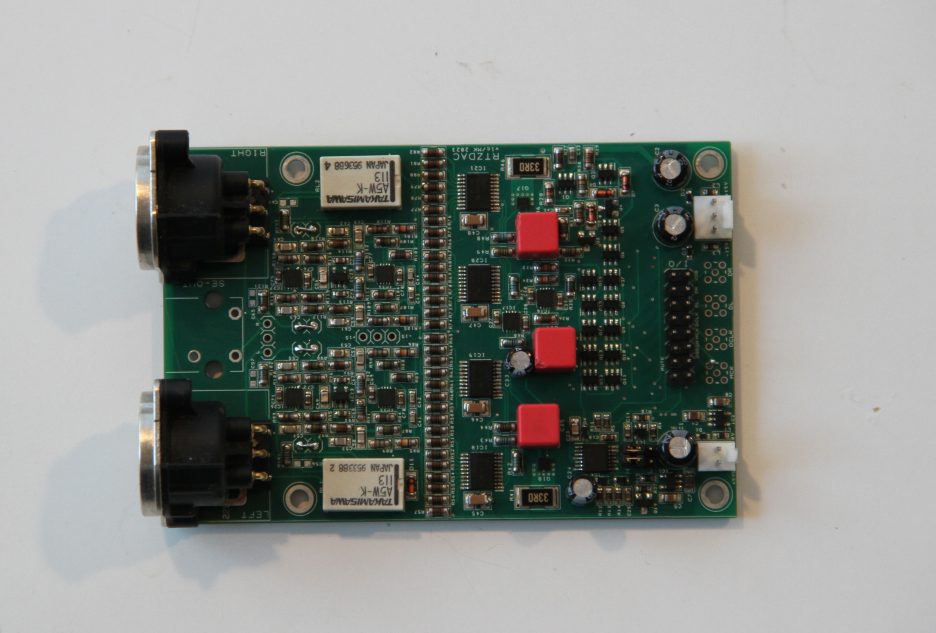
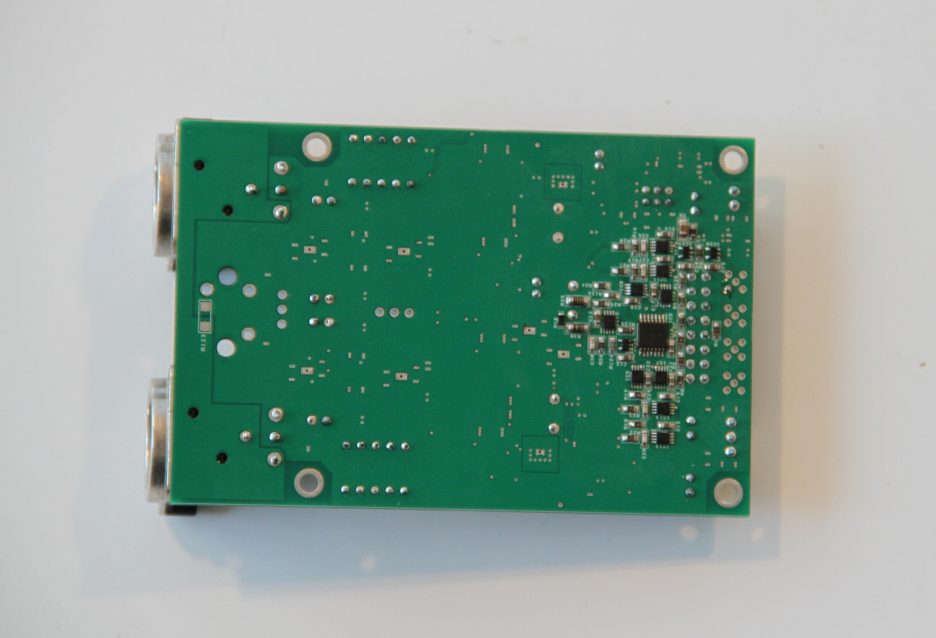
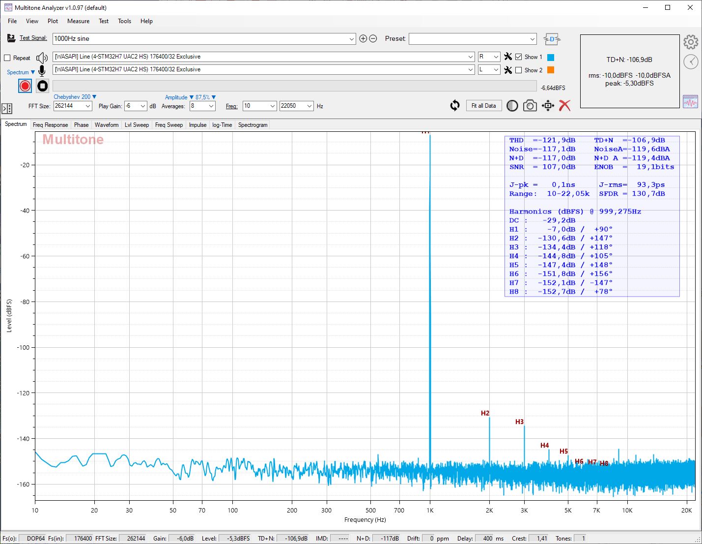
While my aim was to have more balance between channels the performance actually improved also.
Here is SNR at DoP64:
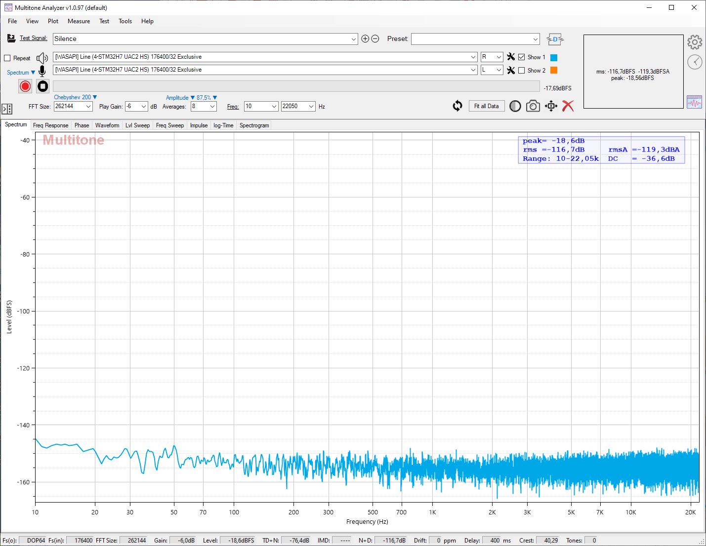
So A-weighted noise improved by about 2.5 dB.
Here is 1kHz at Dop64:
Here are pictures of the new board. I placed the digital section on bottom side, not to have lower noise but mainly for layout symmetricity. This also allowed me to make the board even smaller than the previous (now 67x100mm). Another change was to add a DCLK reclocker (2 flip flops) which also meant that MCK input is needed.
While my aim was to have more balance between channels the performance actually improved also.
Here is SNR at DoP64:
So A-weighted noise improved by about 2.5 dB.
Here is 1kHz at Dop64:
There was some overshoot in the reclocked DCLK so I increased the series termination resistor from 33R to 120R. This improved SNR by 0.5dB.
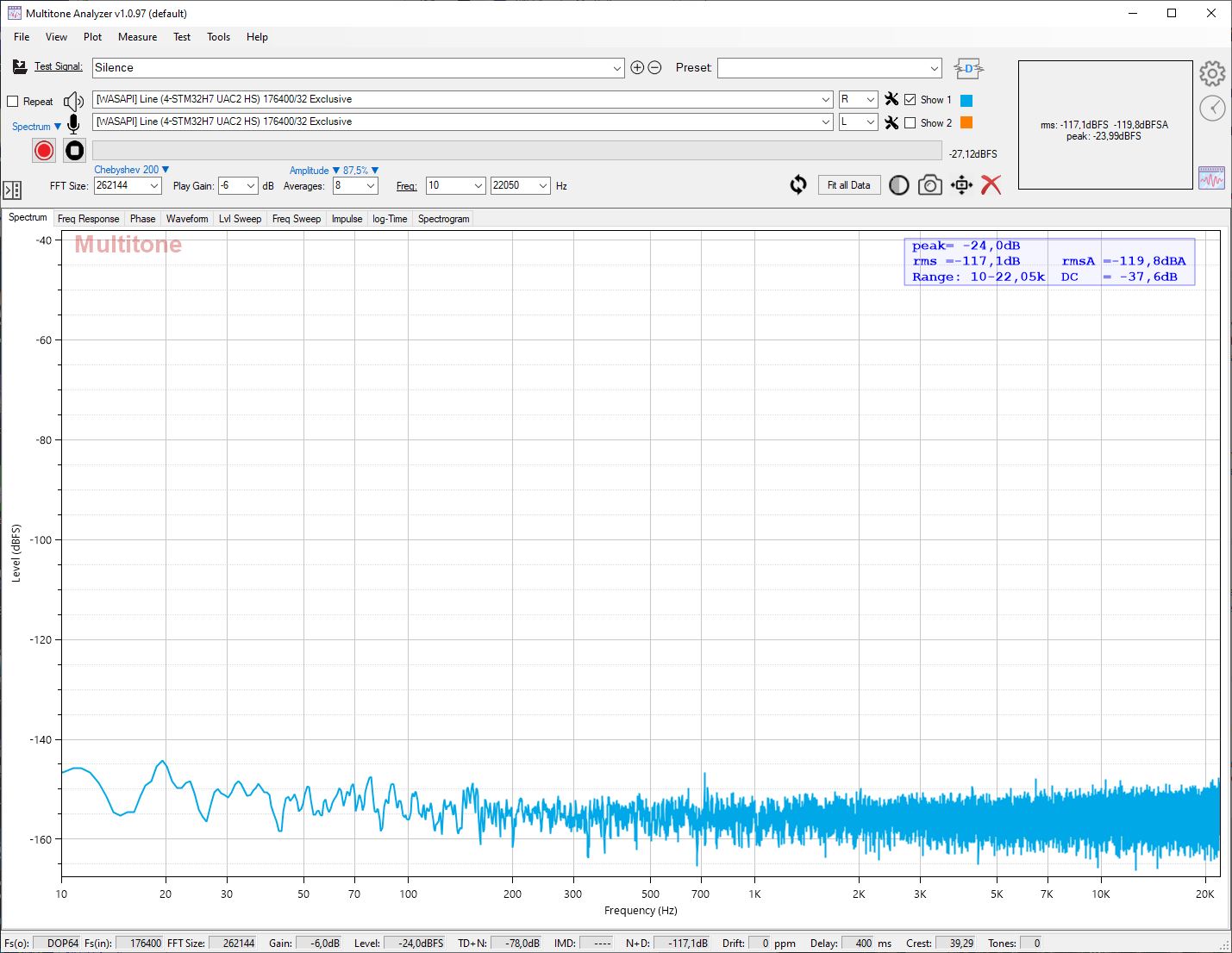
Performance at DoP128 and DoP256 is similar although SNR is a slightly worse (about -118.7dB at DoP128 and -116.8dB at DoP256).
Here is 1kHz DoP256:
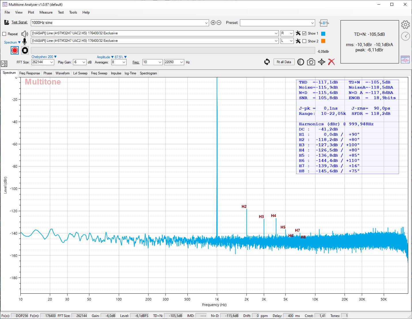
Here is 1kHz DoP256:
For consistency, updated schematic and BOM with the hold time fix included. The only differences are the changed values of R124, R127, R129 and R131.
Attachments
To wrap up my measurements here is 1kHz DoP128 0dBFS with Cosmos APU notch. SINAD of 110.5dB is quite remarkable for "no DAC" DAC.
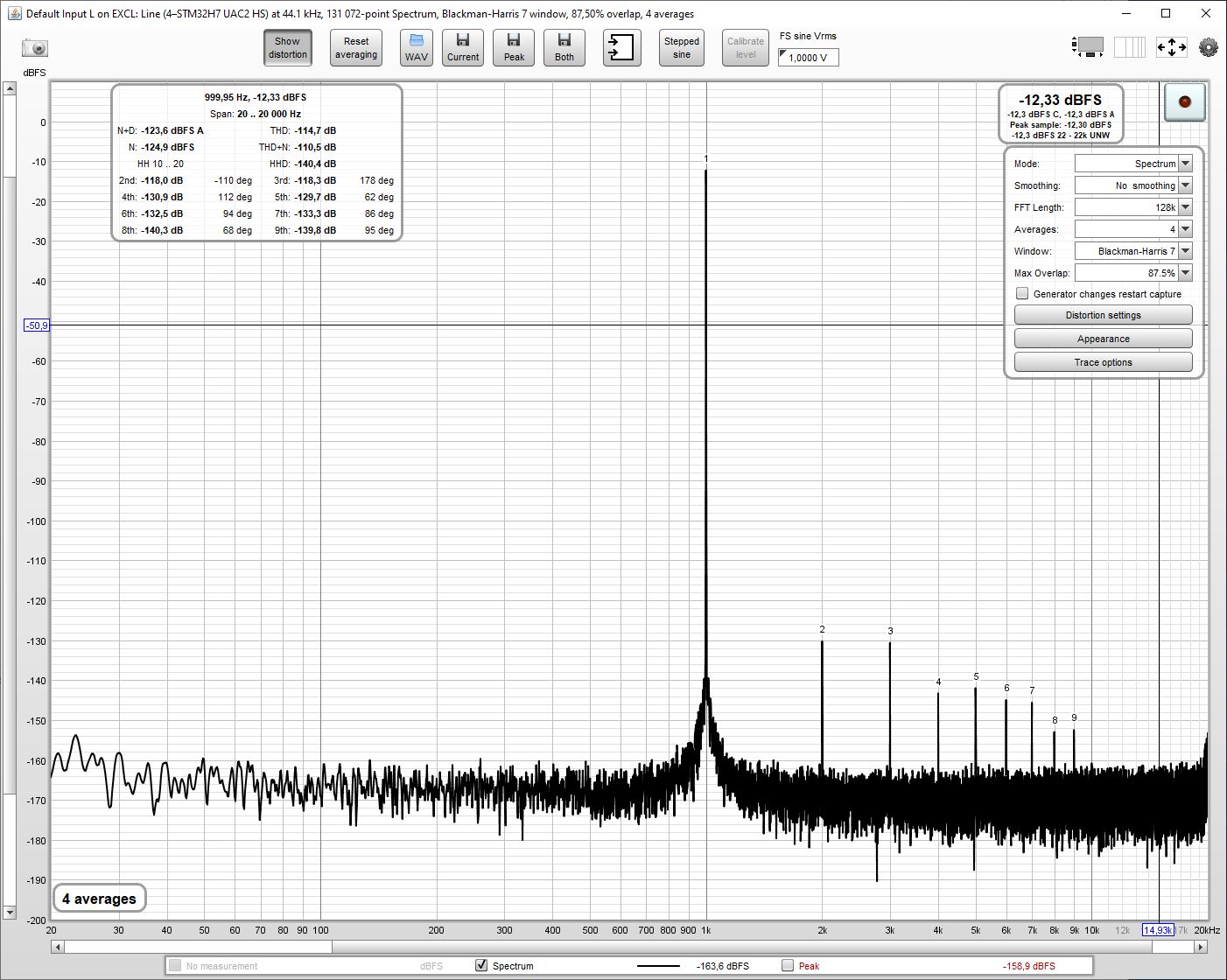
Just as comparison here is Denafrips Ares II:
https://www.audiosciencereview.com/...r2r-usb-dac-dsd-audio-measurements-png.47939/
Just as comparison here is Denafrips Ares II:
https://www.audiosciencereview.com/...r2r-usb-dac-dsd-audio-measurements-png.47939/
As some have already noted soundwise this dac is very good and especially the soundstage seems to be a strong point. But to not get too carried away with subjective superlatives I did some level matched AB testing against my ES9038Q2M (dual mono) and ES9039Q2M dacs using DSD128 as input. ESS dacs were used in sync mode. As usual with more control the differences became very small. On most recordings I could not hear any real difference. However on certain recordings RTZ dac seemed to have slightly wider soundstage. Whether or not that is better depends on subjective preferences.
That has been used here to denote DACs that don't utilize a dedicated DAC chip. Although IMO FPGA-based DACs are borderline cases.Whats is a "No DAC"?
IIUC a 'No DAC' is a more or less passive DSD dac. Two data lines, each one into a passive filter.
https://www.diyaudio.com/community/threads/the-best-dac-is-no-dac.273474/post-4309884
https://www.diyaudio.com/community/threads/the-best-dac-is-no-dac.273474/post-7426408
https://www.diyaudio.com/community/threads/the-best-dac-is-no-dac.273474/post-4309884
https://www.diyaudio.com/community/threads/the-best-dac-is-no-dac.273474/post-7426408
Last edited:
@hazard500 should know, as he/she/it/they came up with the term NoDAC.
https://www.diyaudio.com/community/threads/the-best-dac-is-no-dac.273474/post-4304814
https://www.diyaudio.com/community/threads/the-best-dac-is-no-dac.273474/post-4446944
https://www.diyaudio.com/community/threads/the-best-dac-is-no-dac.273474/post-4304814
https://www.diyaudio.com/community/threads/the-best-dac-is-no-dac.273474/post-4446944
- Home
- Source & Line
- Digital Line Level
- Return-to-zero shift register FIRDAC