Excellent work ! I must try the passive output .
Definitely worth experimenting with the regged supplies I'm finding all make a difference , I currently use 5v shunt for the Firdac , pair of LT1086 wired up for the +/-15v FIRDAC (might change these to shunts) , LM1085 5v for the reclockers pre reg to the LT1763 . I might try a shunt for the reclockers pre reg
Definitely worth experimenting with the regged supplies I'm finding all make a difference , I currently use 5v shunt for the Firdac , pair of LT1086 wired up for the +/-15v FIRDAC (might change these to shunts) , LM1085 5v for the reclockers pre reg to the LT1763 . I might try a shunt for the reclockers pre reg
Hi willing to join here, before order an unwanted 5 MOQ FirDac PCBs, lets me ask if somebody has a leftover FirDac PCB board & stencil. I am from Catalonia (Spain).
Thanks in adv and sorry if inconvenience,
Jordi
Thanks in adv and sorry if inconvenience,
Jordi
Last edited:
Hi Jordi,
I have a spare RTZ DAC pcb. I do have a stencil but I want to hang onto it in case I need it again.
Cheers,
Tony
I have a spare RTZ DAC pcb. I do have a stencil but I want to hang onto it in case I need it again.
Cheers,
Tony
Transistor BC858B,215 is out of stock at Mouser. It seems his closer one is BC858QR, does is allowed as substitute?

Yes, no problem. BC858B-QR is the automotive qualified version of the same transistor.
(I thought for a moment that the package was different, but it isn't; SOT23 and TO-236AB are two different codes for the exact same package.)
(I thought for a moment that the package was different, but it isn't; SOT23 and TO-236AB are two different codes for the exact same package.)
Last edited:
I am thinking about one board per channel with even longer taps, wondering if this is reasonable, also need to modify the power/sense line.
With 3rd order filter, I can still hear the ultrasonic fuzzy noise on some of the music, hope more taps can help, or maybe a 5th order filter.
I have added a new thread for the v15 reclocker.
I can now provide the Gerbers and information to build an interface board that supports a compact connection between JLSounds I2SoverUSB vIII FIO and PCM2DSD with support circuitry hosting 2 x XOs, relays to switch in the correct frequency, re-clocking for the DSD signals and a clock doubler to provide ext_clk to the JLSounds if 22/24Mhz XOs are used.
The design relies heavily on that generously provided by Markw4 and was conceived not as an alternative to his design but to complement it where space was limited and requirements weren't as general.
This is the link to Mark's design...
The design relies heavily on that generously provided by Markw4 and was conceived not as an alternative to his design but to complement it where space was limited and requirements weren't as general.
This is the link to Mark's design...
- Cestrian
- Replies: 91
- Forum: Digital Line Level
Load here
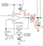
I found one more thing I would like to change: replace R14 with the series connection of an LL4148 and an 8.2 ohm resistor. As is, U1B can pull the supply voltage of U28 and U29 (clocksup_F) negative during power down, when its -15 V supply ramps down slower than its +15 V. I have changed this on my board and checked that everything still works, the schematic and layout are to be updated.
At start-up, the -15 V supply has to reach -0.3 V no later than 180 milliseconds after the +15 V exceeds +5 V. This is related to the common-mode input voltage range of U1A. You could get a too...
At start-up, the -15 V supply has to reach -0.3 V no later than 180 milliseconds after the +15 V exceeds +5 V. This is related to the common-mode input voltage range of U1A. You could get a too...
Hello, I please request for advice, today I do the very first power up to the Firdac board.
After a safely test for the Op Amps. I got 5V. present once R18 removed/ short C8.

I tought Ok and placed the parts back, but no output sound.
Then a quick multimeter test I found BCK input signal is shorted to ground.
Fixed! after realising those U-fl shockets are directional (it was socket P13 'bckin' soldered backwise)
Now better, but only the left channel is playing music. Right one is silent.
Please see atch. screenshot, do is correct my wiring for single ended putput?

I can't see any further bad soldering or bridge visually,
Ah, it is no reclock yet, sound chain is just a healthy stereo DSD2PCM input signal, and passive filter output also reliable.
Thanks in advance,
Jordi
After a safely test for the Op Amps. I got 5V. present once R18 removed/ short C8.

I tought Ok and placed the parts back, but no output sound.
Then a quick multimeter test I found BCK input signal is shorted to ground.
Fixed! after realising those U-fl shockets are directional (it was socket P13 'bckin' soldered backwise)
Now better, but only the left channel is playing music. Right one is silent.
Please see atch. screenshot, do is correct my wiring for single ended putput?

I can't see any further bad soldering or bridge visually,
Ah, it is no reclock yet, sound chain is just a healthy stereo DSD2PCM input signal, and passive filter output also reliable.
Thanks in advance,
Jordi
Jordi,
Do you have an oscilloscope?
Regarding the short at C8, there aren't very many things attached to that node. You either start lifting pins, removing the cap, or maybe cutting traces (in a way so you can solder a jumper over the cut later to fix it). Somehow you need to find the location of the short. Or did you already find the short? Not quite clear on that?
Regarding the u.fl connectors, yes, they can be installed backwards. Usually the signal pin looks a little different than the ground pin on the other side.
So if no shorts now, then you either need a scope or maybe you could try swapping the board's input signal inputs for the left and right channels to see if the sound moves from one channel to the other. If not then it can be pretty hard to find the problem without being able to check some scope signals.
Also, I believe OUTPF is probably the in-phase output signal, not OUTMF. Also, maybe better to look at sheets 3 and 4 at this point. The left and right signals can be seen to be interleaved between shift registers. So the problem may be the digital signal for one channel is not coming into the shift registers. In that case you might need to look at sheet 5.
You are using the inverted sides and left and right appear to be swapped (unless your USB interface has them swapped compared to an Amanero), but yes, you should get sound left and right.
What happens when you use the positive pins, so 2 or 3 and 7 or 8?
What happens when you use the positive pins, so 2 or 3 and 7 or 8?
Yes Mark, I have a digital one at 100Mhz. I can take measurements when free time (not every day.)Jordi,
Do you have an oscilloscope?
Regarding the short at C8, there aren't very many things attached to that node. You either start lifting pins, removing the cap, or maybe cutting traces (in a way so you can solder a jumper over the cut later to fix it). Somehow you need to find the location of the short. Or did you already find the short? Not quite clear on that?
Sorry Mak my bad, limited english, and limited languaje skill alltogether.
I leaved R18 out initially and grounded the R18 / C8 point so that the op-amps see zero at the first power up. Is a trick Cestrian kind gave me in order to ...I quote "...isolate the DAC reference from the downstream ICs (...) Then power up and see what voltage you have on the output of U1A ". I got the same 5V. that Cestrian guessed by just looking to the diagram.
What test points should be useful for me to measure the diferences between channels?Regarding the u.fl connectors, yes, they can be installed backwards. Usually the signal pin looks a little different than the ground pin on the other side.
So if no shorts now, then you either need a scope or maybe you could try swapping the board's input signal inputs for the left and right channels to see if the sound moves from one channel to the other. If not then it can be pretty hard to find the problem without being able to check some scope signals.
Not that easy to swap input channels, as I have the firdac board plugged to the 20 pin DSC interface on PCM2DSD (without cables)
I confirmed now OUTPF (pin 7 in P3 connector_01x11) is much better sounding than OUTMF (pin 10)Also, I believe OUTPF is probably the in-phase output signal, not OUTMF. Also, maybe better to look at sheets 3 and 4 at this point. The left and right signals can be seen to be interleaved between shift registers. So the problem may be the digital signal for one channel is not coming into the shift registers. In that case you might need to look at sheet 5.
I see some interesting test points on those sheets, as time permits, I will post here screenshots from oscilloscope.
Thanks Mark
Thats right Marcel, I noticed just after upload I typed R and L wrong.You are using the inverted sides and left and right appear to be swapped (unless your USB interface has them swapped compared to an Amanero), but yes, you should get sound left and right.
What happens when you use the positive pins, so 2 or 3 and 7 or 8?
Pin 2 is dead.
Using pin 7 improves the sound Vs. pin 10, but still something faulty on this channel. Sound can be harsh before components burn in, but not weak.
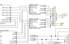
On sheets 3 and 4 of the latest schematic that Marcel posted, the digital non-inverting and inverting signals are outlined in red below (signals to check with a scope):

sdn for the negative or inverting signals for each channel (negative serial data). sd is for the non-inverting or positive outputs (serial data).
Those signals come from sheet 5 of the schematic:

You should make sure those resistor values in the red box are actually 270R.
sdn for the negative or inverting signals for each channel (negative serial data). sd is for the non-inverting or positive outputs (serial data).
Those signals come from sheet 5 of the schematic:
You should make sure those resistor values in the red box are actually 270R.
There are many fault finding measurements you could even do with just a multimeter, a makeshift low-pass filter and some audio equipment, but as you have a good digital oscilloscope, it makes sense to use it.
U7 and U9 require a reference/supply voltage, a clock signal and two data signals to do their job, so you can check if they get all of that. To reduce the risk of shorting things while probing the circuit, I would measure at nearby resistor and capacitor pins rather than directly at the IC pins.
While playing a DSD signal, using your scope and a 1:10 probe, you could check the following voltages, all with respect to ground:
Is there about 5 V on one pin of C19 and C21?
Is there a clock signal of about 5 V peak-peak at twice the bit clock frequency on both pins of R132? It should consist of pulses of about 8 ns long. It's normal when you see a slightly short period, slightly long period, short period, long period and so on.
What do the data signals on both pins of R129 and R131 look like? If you see a signal, could you do a single-shot measurement?
What do you see on R126?
Last edited:
- Home
- Source & Line
- Digital Line Level
- Return-to-zero shift register FIRDAC