No, only 28 euros. But if the board is 100x100mm (or less) 4-layer is 6.5euros, 6-layer 56 euros and 8-layer 80 euros (+ shipping & taxes). That is one of the reasons I keep my boards small. I have rarely managed to design complex boards without iterations so costs can mount up at prototyping. This is only a hobby for me so I don't do mass production.And presumably 45 Euro's for 4-Layer?
IMHO, there is no replacement for displacement, ahm, layers. For designs like this I'd certainly use 6 or 8 layers as the cost penalty is minimal these days. Of course many layers alone don't make a good PCB design but it let's you avoid making compromises which could turn out worse then expected.

As I said depending on the board size the cost penalty is not minimal. Another issue is that low cost PCB manufacturers do not support blind and buried vias which are quite essential to get full benefits of 6- or 8-layers.For designs like this I'd certainly use 6 or 8 layers as the cost penalty is minimal these days.
Minimal is relative of course, but I found it to be so in the light of total project costs and time invested, even for DIY or prototyping one-offs and even for larger than the 100x100 "brickwall". Only minimum order qty of 5 or 10 pcs drives cost in the end for one-offs.As I said depending on the board size the cost penalty is not minimal. Another issue is that low cost PCB manufacturers do not support blind and buried vias which are quite essential to get full benefits of 6- or 8-layers.
Agreed, blind/buried vias would be ideal and JLCPCB etc don't do them, but with rings removed on unconnected layers (including the outer layers) I find the real-estate penalty non-significant -- main exceptions would be larger BGAs and ultra-high density designs in general. Much more important is copper-capped vias so one can use via-in-pad.
It is not only about real-estate. There are other benefits to blind and buried vias such as better signal integrity and more flexible component placement & routing.I find the real-estate penalty non-significant
I have rarely managed to design complex boards without iterations so costs can mount up at prototyping.
Same here.
Generally speaking otherwise, I value my time more than money. Using 6-8 layers allows much better layout much faster, the improvement is as large as going from 2 to 4 Layers.
As for reversing the signal and gnd/pwr layers in 4-Layers etc., may I recommend some reading:
https://hott.shielddigitaldesign.com/techtips/pcb-stack-up-2.html
https://hott.shielddigitaldesign.com/techtips/pcb-stack-up-3.html
https://hott.shielddigitaldesign.com/techtips/pcb-stack-up-4.html
https://hott.shielddigitaldesign.com/techtips/pcb-stack-up-6.html
Some additional benefit I found is that having this many planes, your impedance's properly preset in the EDA, drawing the PCB becomes pretty simple. Do the right stack-up etc. do the presets, mark up impedance controlled lines and after physical placement of critical parts you might be able to run the auto place and router and get somewhere where you dont have to make a lot of changes.
Again, placing a high speed signal line on top is an understandable tendency.
However running it buried between GND & VCC for wherever the power domains are the same, ensures direct returns for all currents. See here:
https://hott.shielddigitaldesign.com/pdf_files/Digital Logic Current Flow.pdf
Stack-up would be GND SIGNAL1 VCC1 VCC2 SIGNAL2 GND with identical thickness of core and prepreg for a purely digital mixed signal setup. If size is not a constraint then one sided placement of parts may be perfect.
And as a bonus Mr. Ott on decoupling...
https://hott.shielddigitaldesign.com/techtips/decoupling.html
I would still, however propose that greatest immediate benefit could be realised by replacing two 74XXX574 with 1pcs of 74XXX16374 in TSSSOP case.
The signal lines between pins will be sufficiently short to disregard impedance control. The absolutely symmetrical layout of the IC should fulfil all of MvG's requirements for matching etc., realistically compared to the parasitic's of the IC package even in TSSOP format, on die parasitic's will pale in comparison.
Combining this with a solid ground plane under the IC and running signals on the inside layer with the second inside layer used for VCC for the DAC will maximise the performance gains for the design.
The only other option to create an even greater separation between logic supplies and Logic Induced Modulation (LIM) would be to separate the delay chain and the output switching, for example by running super fast 3.3V logic for the delay chain (say 74LVC16374) running on the global 3.3V power domain and a 3.3V input compatible 5V PSU output latch like 74ACT16374 for the actual output.
Use multiple 0.1% tolerance resistors in series (or parallel) to improve tolerance (e.g. 3.01kOhm 1% -> 3 X 1kOhm 0.1% or better
The output latch would get the direct bit clock clock, while the delay chain get's an inverted clock, preferably not ~50% duty cycle but instead with a shorter, ~25% duty cycle for the "H" following the latching edge of the output stage clock. Only the timing of the clock latching the temporary state of the delay chain into the outputs will be critical. For all else we gain a much greater resilience to sub-ideal conditions
This suggests a "dirty logic" 3.3V Power domain covering everything up to and including the delay chains, a DAC analogue supply Domain strictly driving the output latch and local crystal clock which is derived from the same source as the 5V supply, perhaps with the clock circuitry placed symmetrically in-between the two DAC's.
If we add a PLL based clock cleaner/multiplier to use the original BCK as clock and generates a (say) 4X BCK (Si5315A/17A at 60Hz BW and perhaps - we can call it Femto Glock) we can use some basic logic to derive the 25% DC output latch clock and a 75% DC RTZ clock.
All of that from a BCK/DSDL/DSDR input which requires neither synchronisation nor low jitter for excellent DAC performance. Input isolation is optional.
It would still very much be Marcel's RTZ DAC, however with IMNSHO an overall much improved situation regarding LIM, which may or may not be a contributing factor regarding all that noisy and harmonic and disharmonic Jazz and over 3dB more output.
Again, just suggesting ways to potentially (maybe with a reasonable expectation of actually) improve a very interesting design.
Thor
And yes, in principle the hardware improvements I suggest are just as applicable to NRZ or RTO FIR DAC's, where, together with LVC output logic the closely matched rise & fall times will significantly limit ISI related problems and combined with a true balanced design would convert the H2 caused by ISI to common mode and thus add a lot of H2 suppression.
realistically compared to the parasitic's of the IC package even in TSSOP format, on die parasitic's will pale in comparison.
Like I wrote in a PM a couple of months ago, it's more the on-chip resistance than the inductance I worry about. (I have seen cases where on-chip trace inductance caused problems, but that was usually at frequencies of 1 GHz and above.) Metal traces on a chip are normally much thinner and narrower than those on a PCB, even the wide supply and ground traces to output cells.
It is not only about real-estate. There are other benefits to blind and buried vias such as better signal integrity and more flexible component placement & routing.
I would very much like buried via's, but they really are disliked by even quite high end, high competence industrial PCB suppliers.
The solution is to change the stack-up so that that the resultant stubs are minimised for .
Then again, on a 1.2mm thick PCB the absolutely worst case stub from a via not removed would be 1.2mm. At 70% C the rise time needed to have any material problem with this will be around 0.6nS or less, which I think we are not required to worry about in our applications.
So a 1.2mm 6-layer PCB with optimised stack-up should be fine, minimised stubs should be 0.2mm, worst case 1mm.
Thor
Like I wrote in a PM a couple of months ago, it's more the on-chip resistance than the inductance I worry about.
I would still expect to have an improved situation in a 16 Bit bus driver with tightly specified output to output skew and the layout we see over the classic 74 TTL style layout. Do you disagree that this is at the least a reasonable expectation?
Thor
Not sure if all the focus is not missing something here. When do we get to looking at how Vref is affecting the sound? How about the effects of how the doubled clock is being generated? I'll be those things have as much or more effect on the sound as does all the focus on little switching glitches. Also, Cestrian already built an output stage board with OPA1632 and says the mushy sound is now gone.
Regarding the mushy sound, I agree that's what the original output stage board sounded like to me as well. Bypassing the last stage and slowing down the CM servo, both helped reduce the mush but not enough for me. Maybe what Cestrian built is good enough (given he then passes the output signals though transformers)?
Then once we fix all that other stuff, maybe we will hear an audible difference from rerouting shift register bypass currents? Probably we would, at least IME it seems rather likely.
Last edited:
Reply to post #2809:
So far bohrok2610's measurements seem to indicate that the filter is the performance bottleneck, at least for low-level distortion due to intermodulation between out-of-band signals, but assuming that that will be fixed:
There is a good chance that an SN74ACT16374A would outperform two SN74LV574A's, though I can't be sure about that. On the positive side, the supply and ground pin-out is definitely better, and looking at the symmetry of the pin-out, chances are that the whole chip is laid out symmetrically. That's very nice for matching. The output resistance is also lower.
On the other side, the chip is somewhat slower, and no one knows which has least 1/f noise.
At 25 degrees Celsius and 4.5 V unless otherwise noted:
SN74ACT16374A:
VOL max. 0.36 V at 24 mA -> max. 15 ohm
VCC - VOH max. 0.56 V at 24 mA -> max. 23.333... ohm
VOL max. 0.44 V at 24 mA over temperature -> max. 18.333... ohm
VCC - VOH max. 0.7 V at 24 mA over temperature -> max. 29.1666... ohm
tPLH clock to output 5.1 ns min., 8.8 ns typ., 10.9 ns max.
tPHL clock to output 5.3 ns min., 8.8 ns typ., 10.9 ns max.
I haven't seen an explicit skew specification in the TI datasheet, by the way.
SN74LV574A:
VOL max. 0.55 V at 16 mA over temperature -> max. 34.375 ohm
VCC - VOH max. 0.7 V at 16 mA -> max. 43.75 ohm
tPLH clock to output 4.8 ns typ., 8.6 ns max.
tPHL clock to output 4.8 ns typ., 8.6 ns max.
When you drive SN74ACT16374A inputs from a dirty 3.3 V domain, the high inputs will draw an overlap current from the 5 V reference that depends on the momentary voltage at the dirty 3.3 V.
I don't see the advantage of separating the shift register from the output registers, except maybe that the load on the last flip-flop will then better match that of its colleagues. The data clocked into the output registers will be the same, no matter whether you use them only as output registers or also as a shift register.
Regarding return to high impedance (or return to off) rather than return to zero, I think it will be difficult to keep intersymbol interference under control with such a scheme.
The plot in post #2696 shows that a +/- 1 ppm change of the bit weight depending on the previous bit is enough to produce about the same intermodulation products in the audio band as the present DAC and filter do. Now suppose a three-state output with a capacitance of 5 pF were connected to an ideal virtual ground via a 3 kohm resistor. In the high-impedance state, the discharge time constant would then be 15 ns. If there were 45 ns available for discharging, about half a DSD256 bit clock period, that would only be three time constants. That is, there would be almost 5 % of the previous bit voltage left at the start of the new bit, and that should disturb the weight of the new bit by less than 1 ppm.
With a nonideal virtual ground or no virtual ground at all, the voltage the output would settle to in its high-impedance phase would depend on more previous bits, presumably making things worse.
Hi all ... just a "brief" comment ...
As I mentioned in an earlier post I have made three versions of the RTZ DAC with various routings for the clock, FF & output resistors. I have also tried different decoupling capacitors while measuring the differences. Much to my surprise they measure almost the same (~- 112 dB THD with close to the same harmonics' profile) which have had me thinking about why that may be ...
And assuming I have not made any actual mistakes (it does not look like it, I would say), and considering @bohrok2610's solution, it seems that there may be these possible explanations:
1. I reckon @bohrok2610 uses the TVSOP package (?) whereas for convenience I chose to use the TSSOP package in all three layouts. Although the package inductance differences between the pins of these two packages are not "huge" this could be an explanation for the THD differences between the layouts.
2. @bohrok2610 uses (mini?)melf resistors which I reckon may have lower load-dependent distortion. In all three versions I used the RR1220s from Susumu (to my memory the ones Marcel listed in the BOM? Anyway 100mW, 0805). The Susumus might distort more (?), however, I also use these resistors in another context where they see a higher load and the distortion is at a >-125 dB (THD) level. So I wouldn't consider this to be the reason.
3. @bohrok2610 appears to connect the decoupling capacitor's VCC pole to an underlying VCC trace/plane - and then from this trace/plane to the VCC pins on the LV574 FFs (correct?):
https://www.diyaudio.com/community/threads/the-best-dac-is-no-dac.273474/page-116#post-7423010
If this is so, I reckon this would "tie" the LV574s' VCC pins to identical VCC trace/plane potentials (excluding the inductance/impedance of the VCC plane/trace itself which, however, would likely be quite low, maybe ~40 pH and sub-milliohms (?) and the inductances of the via pins going from the VCC pins to the VCC trace/plane). However, it would also add "two" via inductances from each decoupling capacitor to each VCC pin ... (I write "two" because each decoupling capacitor is connected to the VCC trace/plane with three vias thus reducing the inductance (and resistance) of this connection) ...
4. @bohrok2610 appears to use a smaller size decoupling capacitor which may/might also imply a lower inductance of this capacitor (and possibly a better decoupling of the VCC pin noise).
Just some observations and thoughts.
Additionally, I have been wondering how the crosstalk between the output resistors may affect the performance? This crosstalk might/may be "considerable" ... assuming a 1.5 ns rise/fall time it would be on the order of some -30 dB (according to Saturn PCB Design). But maybe because there is a "rise & fall edge situation" between the adjacent output resistors this is balanced out? However, even if this is so, the "outermost" resistors - i.e. the resistors towards the ends of the shift registers - would not see exactly the same crosstalk field "balancing" ...
@ThorstenL : Interesting information about PCB stackup, thanks for mentioning them. One thought here: Since the identical potential and impedance of the VCC and GND planes depend on the even - and efficient - decoupling at all frequencies between these planes - i.e. a fully linear decoupling capacitor arrangement between these planes - will you not see a frequency-dependent & thus uneven trace impedance on the VCC and GND sides of a signal trace being placed between a VCC & GND plane?
Well, my current thoughts on this. Have a fine day all of you ...
Cheers, Jesper
I use VSSOP for 74LVC1G74, 74LVC2G86 and 74LVC2G32. TSSOP for other ICs. I use smaller package just for space savings, not performance. Although smaller board size should be beneficial due to shorter traces and smaller loop areas. I also have digital circuit on bottom side and analog circuit & Vref on top side. This may help to reduce noise.1. I reckon @bohrok2610 uses the TVSOP package (?) whereas for convenience I chose to use the TSSOP package in all three layouts. Although the package inductance differences between the pins of these two packages are not "huge" this could be an explanation for the THD differences between the layouts.
The impact of summing resistors on THD should be very small.2. @bohrok2610 uses (mini?)melf resistors which I reckon may have lower load-dependent distortion. In all three versions I used the RR1220s from Susumu (to my memory the ones Marcel listed in the BOM? Anyway 100mW, 0805). The Susumus might distort more (?), however, I also use these resistors in another context where they see a higher load and the distortion is at a >-125 dB (THD) level. So I wouldn't consider this to be the reason.
I don't think this matters much on THD.3. @bohrok2610 appears to connect the decoupling capacitor's VCC pole to an underlying VCC trace/plane - and then from this trace/plane to the VCC pins on the LV574 FFs (correct?):
https://www.diyaudio.com/community/threads/the-best-dac-is-no-dac.273474/page-116#post-7423010
If this is so, I reckon this would "tie" the LV574s' VCC pins to identical VCC trace/plane potentials (excluding the inductance/impedance of the VCC plane/trace itself which, however, would likely be quite low, maybe ~40 pH and sub-milliohms (?) and the inductances of the via pins going from the VCC pins to the VCC trace/plane). However, it would also add "two" via inductances from each decoupling capacitor to each VCC pin ... (I write "two" because each decoupling capacitor is connected to the VCC trace/plane with three vias thus reducing the inductance (and resistance) of this connection) ...
I use 0603 X7R 100nf for all ICs except for shift registers. Again this shouldn't impact THD.4. @bohrok2610 appears to use a smaller size decoupling capacitor which may/might also imply a lower inductance of this capacitor (and possibly a better decoupling of the VCC pin noise).
I assume you are concerned about THD and not THD+N as noise is what mostly impacts the latter. Clean clocks are critical for low noise. Also most of my layout and component choices were aimed at lowering noise, not THD. My guess is that for lower THD you should focus more on the output stage.
If I may chime in...@ThorstenL : Interesting information about PCB stackup, thanks for mentioning them. One thought here: Since the identical potential and impedance of the VCC and GND planes depend on the even - and efficient - decoupling at all frequencies between these planes - i.e. a fully linear decoupling capacitor arrangement between these planes - will you not see a frequency-dependent & thus uneven trace impedance on the VCC and GND sides of a signal trace being placed between a VCC & GND plane?
One trick is to treat all supply/GND planes as one and the same thing, impedance-wise and for return current paths, just sometimes separated by a DC offset. They must connect to each other in a distributed fashion. For two GNDs to connect you use vias, and when there is a DC offset you insert a DC blocking cap ("decoupling"). Same for any return path vias when a track switches layers. When there is a DC offset between the return path planes again you insert a series DC-blocking cap in the return path.
Not sure if all the focus is not missing something here. When do we get to looking at how Vref is affecting the sound?
Let me rephrase "Vref" to DAC Power Supply.
It means it is impacted by the analogue signal and any logic noise that "get's past" decoupling.
How about the effects of how the doubled clock is being generated?
I think this was discussed, using a local crystal clock and synchronising the source to it was @bohrok2610 's solution, something I agreed with.
In order to retain a simple "stand alone" DAC without worrying about cIock domains and synchronisation I suggested a Si5317 DPLL clock cleaner, which can be set to 60Hz bandwidth and offers sub-ps RMS jitter above a few 100Hz. One might want to play with the hardware settings to see if it possible to trick the IC into lower bandwidth while retaining low jitter.
As bonus, we can use Si5317 as clock multiplier to (say) 4 X input BCK to allow RTZ with 75% duty cycle as opposed to 50%.
I'll be those things have as much or more effect on the sound as does all the focus on little switching glitches.
Possibly.
Also, Cestrian already built an output stage board with OPA1632 and says the mushy sound is now gone.
So it suggests to me (circumstantial evidence) that the problem is attributable to a combination of the OPA2210's common emitter output stage and intermodulation of switching noise at this point. So OPA1632 or my suggestion of "Birt" compound with a hybrid adding a low noise OPA with a differential CFB OPA outpput would look very likely good solutions.
Then once we fix all that other stuff, maybe we will hear an audible difference from rerouting shift register bypass currents? Probably we would, at least IME it seems rather likely.
Ditto.
So far bohrok2610's measurements seem to indicate that the filter is the performance bottleneck, at least for low-level distortion due to intermodulation between out-of-band signals, but assuming that that will be fixed
My concern is that at least in theory we should not have this. FIR lowpass and inherent RC filtering with 3uS turnover (~53kHz) should keep supersonic problems at arms length.
If additional LC filtering helps, we need to consider that we have a fidelity impairment risk upfront in our DAC structure, which is unexpected actualised with certain types of analogue stages.
There is a good chance that an SN74ACT16374A would outperform two SN74LV574A's, though I can't be sure about that.
16374 Bus Latches come in many different logic families.
On the positive side, the supply and ground pin-out is definitely better, and looking at the symmetry of the pin-out, chances are that the whole chip is laid out symmetrically.
Knowing human nature this is not certainty, but likely.
On the other side, the chip is somewhat slower, and no one knows which has least 1/f noise.
I suspect 1/f noise is family dependent.
I haven't seen an explicit skew specification in the TI datasheet, by the way.
There are extended application notes (I seem to remember sharing some here and others with you? Maybe not) that go into this in detail for different logic families. Fascinating reading heavy on grap[hs..
When you drive SN74ACT16374A inputs from a dirty 3.3 V domain, the high inputs will draw an overlap current from the 5 V reference that depends on the momentary voltage at the dirty 3.3 V.
You mean through the P-Channel device's Ciss? It is probably worth slowing the edges here to minimise this feedthrough.
I don't see the advantage of separating the shift register from the output registers, except maybe that the load on the last flip-flop will then better match that of its colleagues. The data clocked into the output registers will be the same, no matter whether you use them only as output registers or also as a shift register.
Correct. Signal is not really affected as such.
HOWEVER, the current in the 5V DAC Supply will differ.
If we slow edges of the data lines to guard against feedthrough and have a complementary layout and signals we can expect substantially less "spikey" current on the reference.
There is just less swicherigerdiroo going on on that chip. As said, a chip with dual supply domains for input and output we can improve the situation a little more.
What is more, done right, the DAC will latch the data on the "idle" cycle of all the other logic and even the logic on the input's would have settled any ground/supply bounce by the time we do the DAC update. It should deal with jitter produced LIM and minimise it to least possible. By the time we get ground/supply bounce from updating the DAC storage register the clock edge will have already been registered and the DAC update has begun, while all other circuitry has already settled.
Regarding return to high impedance (or return to off) rather than return to zero, I think it will be difficult to keep intersymbol interference under control with such a scheme.
Remains to be seen.
With a nonideal virtual ground or no virtual ground at all, the voltage the output would settle to in its high-impedance phase would depend on more previous bits, presumably making things worse.
But our output always depends on previous bit's. The question is, will the averaged errors even out, the way RTZ allows for uneven rise & fall time.
1. I reckon @bohrok2610 uses the TVSOP package (?) whereas for convenience I chose to use the TSSOP package in all three layouts. Although the package inductance differences between the pins of these two packages are not "huge" this could be an explanation for the THD differences between the layouts.
Could be, trying a 16 Bit part may be a "hack". Personally I stick to TSSOP simply from a supply chain view.
4. @bohrok2610 appears to use a smaller size decoupling capacitor which may/might also imply a lower inductance of this capacitor (and possibly a better decoupling of the VCC pin noise).
In systems with full ground and power planes usually the determining factor for bypassing are the pins, PCB Pads and via's, the planes have enough capacitance to swamp out any sensible bypass Cap's inductance.
@ThorstenL : Interesting information about PCB stackup, thanks for mentioning them. One thought here: Since the identical potential and impedance of the VCC and GND planes depend on the even - and efficient - decoupling at all frequencies between these planes - i.e. a fully linear decoupling capacitor arrangement between these planes - will you not see a frequency-dependent & thus uneven trace impedance on the VCC and GND sides of a signal trace being placed between a VCC & GND plane?
You seem to miss the point. The concept's of ground are fiction.
If we look at an Inverter, the reference point for the N-Channel is Vss (aka "GND") and when it pulls an input and a strip-line low the current return path is via the Vss power plane (aka Ground Plane). The reference point for the P-Channel is Vcc (aka "PWR") and when it pulls an input and a strip-line high the current return path is via the Vcc pin.
So depending on the PCB structure this current either returns via a bypass capacitor and the ground plane and another bypass capacitor (as we do not have a contiguous Power plane surrounding the signal line) or via our Vcc power plane.
It is all about current loops.
Incidentally, if there is enough space, the following stack-up allows something near 6-layer performance on 4 layers.
Top -> Components + GND
Int1 -> Signal 1 / Power 2
Int2 -> Signal 2 / Power 1
Bot -> (Components +) GND
It requires a lot of layout discipline, as we need a "as uninterrupted as possible" power plane on a layer that also handles routing. It is doable, however it is often challenging.
That why my default now is:
Top -> Components + GND
Int1 -> Signal 1
Int2 -> Power 1
Int3 -> Power 2
Int4 -> Signal 2
Bot -> (Components +) GND
Or:
Top -> Components + GND
Int1 -> Signal 1 / Analog
Int2 -> Power 1 / Analog Power +
Int3 -> Power 2 / Analog Power -
Int4 -> Signal 2 / Analog
Bot -> (Components +) GND
Or:
Top -> Components + GND
Int1 -> Signal 1 / Signal 3 / Analog
Int2 -> Power 1 / Power 3 / Analog Power +
Int3 -> Power 2 / Power 4 / Analog Power -
Int4 -> Signal 2 / Signal 4 / Analog
Bot -> (Components +) GND
In this last case Power 1 may be 1.2V core for FPGA, XMOS etc. or split up into 1.2/1.8/2.5V sections per IC depending on Vcc Core demands. Signal 1 would be all signal lines operating at core level and/or uncritical signals.
Power 3 on the same layer might be the DAC Vcc and Signal 3 would be "DAC internal" or again "uncritical".
Power 2 would be the common I/O Power (often 3.3V) and Signal 2 all critical signal wiring referencing to Power 2.
Power 4 could be for example the clock section conceivably with drivers that isolate the Power 2 domain clock tree from the DAC in the Power 4 domain.
Layout would divide into DAC sections L/R, clock in-between the DAC's and finally a large "dirty digital" section.
Going 8 layer is desirable for designs with a complex and timing critical clock tree, especially where devices driven by the clock are in a different clock domain.
By dedicating one layer (say top) to key clocks and ground-fill and the next layer to ground we create a situation where EMC emissions are increased compared to buried lines, but we have highly consistent behaviour as there will no gap's in power planes between power domains. That gives
Top -> Components + CLK (+ GND-Fill)
Int1 -> GND
Int2 -> Signal 1 / Signal 3 / Analog
Int3 -> Power 1 / Power 3 / Analog Power +
Int4 -> Power 2 / Power 4 / Analog Power -
Int5 -> Signal 2 / Signal 4 / Analog
Int6 -> GND
Bot -> (Components +) low speed routing (+ GND-Fill)
Having a solid ground under each high speed IC is still desirable in this setup.
Thor
You mean through the P-Channel device's Ciss?
That also contributes, but I meant through the source follower action of the PMOS.
The simplest way to make a TTL compatible input on a 5 V CMOS chip is just to scale the width-length ratios of the input inverter a bit, but with a PMOS threshold voltage of about -0.7 V, you then essentially have a PMOS source follower from the input to the 5 V reference supply for any input voltage from the switching point to 4.3 V.
Hi all,
& thanks for your feedbacks!
@bohrok2610 : Hmmm ... well, thanks for clarifying although it leaves me puzzled as to what is causing this higher THD in these three layouts. I do not think it is the output stage as the very same stage (Marcel's, without CM circuitry, on a good day clock-wise goes to - 127 dB THD in another DSD DAC). And I actually think the layout(s) are good each in its own respect ... Yet, given that the THD is higher in almost the same way, I reckon some kind of systematic phenomenon is going on ... Anyway, thanks for your helpful feedback!
@KSTR & ThorstenL : Thank you also for your feedbacks ... I suppose there are many ways of doing things depending on one's purposes and preferences ... I think I will let your comments simmer and see how they may inspire my thinking about this ...
Incidentally, I actually do not place that much emphasis on THD figures ... I just find that for an otherwise sensible/"identical" circuitry it may tell something about the "correctness" of the circuitry and changes I make to this circuitry (not intending to elaborate on this - I know there are many fine views on this subject).
Cheers, Jesper
Hmmmm....That also contributes, but I meant through the source follower action of the PMOS.
View attachment 1299510
The simplest way to make a TTL compatible input on a 5 V CMOS chip is just to scale the width-length ratios of the input inverter a bit, but with a PMOS threshold voltage of about -0.7 V, you then essentially have a PMOS source follower from the input to the 5 V reference supply for any input voltage from the switching point to 4.3 V.
AHC/AHCT Designer’s Guide September 1998
If I read this right, the PMOS appears to have a threshold of 4.5V - 1.4V .... 5.5V - 1.6V not 0.7V.
If we have the P-Channel turned on while the N-Channel is also on, we see significant cross-conduction. So I have my doubts that the P-Channel really has 0.7V Threshold and is conducting full on at the the same time as the N-Channel is conducting.
Instead of having this "always on" P-Channel (as it never turns off until you exceed 4.3V) which seems counter productive and would means in "H" there is always current conduction, instead there is a separate hysteresis circuit with a very weak P-MOS pull-up that is enabled if the output is High.
Now, perhaps TI saved the 3 helper fet's and instead make the upper transistor conduct slight, but that would give a very weak pull-up.
So I find the "source follower to +5V" questionable.
I will instead presume instead a P-Channel with ~ 3V Gate threshold, meaning the inpout voltage has to be below 1.5V for the P-Channel to turn on.
Do you have any reference for this that illustrates this to the contrary of my Presumption?
Thor
Last edited:
An alternative Passive Filter.
I first simulated the Firdac connected to a 4th order passive Butterworth filter @80Khz matching the 376,25 output impedance, but was not happy with the suppression in the Mhz region from shift-register's from input to its output , most likely because the filter started with an inductor.
That's why I then prefiltered the Firdac's output with a cap, followed by a buffer. This already gave a solid improvement.
But Marcel pointed me in the right direction to either reverse the 4th order filter having a cap at it's input or use a 5th order passive filter, starting with a cap and making at the same the buffer obsolete, so that's what I did.
Bohrok did a suggestion for this passive 5th order filter with 1.8mH inductors having a low series resistance that are readily available from Mouser.
The input cap for this filter would have been 2.2nF, but I used a slightly larger 3.3nF input cap with 1.2mH inductors.
Inductors and caps values can easily be changed into other values by multiplying the inductors by X and the caps by 1/X.
In the simulation three signals were compared, 1) the shift-register's input signal, 2) It's he output at the eight resistor summing point and 3) the signal at the filters output.
To be able to compare suppression in absolute sense, these signals had to be corrected with a factor,
The maximum versus minimum output from an unloaded Firdac's summing point is 3/8*4.5Volt versus 1/8*4.5Volt, a difference of 1.125Volt or 0.398Vrms for a sine wave.
Since the used passive Filter with 376.25R termination divides that output on the summing point by two, the level at this point has to be multiplied by 2/0.398 = 5.03 to get a 0dB input signal at 0dB level in the simulation.
With the same calculation can be found that the shiftregister's input signal with 1Volt logic has to be multiplied by 11.3 and the DM signal at the filters output by 2.51.
That's what the first attachment is showing for the three different .dsf files that were used, resp:
a 0dB@1Khz converted by Jriver, a -60db@1Khz provided by Bohrok and a file from Marcel with a DC offset of ca. 8mV.
In the attached images I referred to then as JR 0dB, Boh -60dB and Mar +8mV.
With JR 0dB and Boh -60dB, the levels of the 1Khz signals line up perfectly, proving that the multiplication factors are correct.
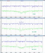
In al images, also the next ones, Blue refers to the Firdac's shiftregister's input signal, Green to its summing point and Red to the 5th order filter output, in the simulation still terminated with 376.25R and without output amp.
Sampling was done with 1Ghz to prevent as much as possible aliases polluting the FFT spectrum, but nevertheless the Blue input signal in the audio band is still visibly somewhat polluted.
The second attachement is showing an image from the same spectrum but now magnified from 0.5 fs to 1.5 fs.
Quite obvious is that the JRiver converted file has no spectral peaks around 0.5 fs and 1.5 fs
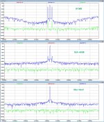
Third to fifth attachment show the further magnified spectrum around resp. 0.5 fs, fs and 1,5 fs, all with a 5Khz/div on the horizontal axis.
Here it is becoming clearly visible what signals on the Firdac's summing point are causing trouble with the Op-Amp filters.
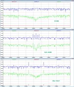
A complete filter including output amp, bringing the 0dB digital recorded level to 2Vrms out, is in the sixth attachment.
This time slightly corrected for the ca. 4R output impedance of the combined eight shiftregisters, bringing the impedance to 380R.
Finally to recapitulate, the noise produced by the equivalent Firdac as a voltage source with a 376,25R output resistance is 15nV/rtHz.
The OPA 2210 filter solution produces an equivalent input noise including the 376,25R resistor 13.6nV/rtHz RTI.
For the complete filter in the last attachment, but also including the 376.25R input, this is 7.2nV/rtHz RTI.
This passive filter followed by a level shifting and DC correcting op-amp solution has the potential to lower the overall S/N ratio by almost 1.7dB and because no feedback mechanism is involved directly after the summing point in the passive filter, no spectral lines in the audio spectrum above -200dB will appear such as suggested by the simulations.
Hans
I first simulated the Firdac connected to a 4th order passive Butterworth filter @80Khz matching the 376,25 output impedance, but was not happy with the suppression in the Mhz region from shift-register's from input to its output , most likely because the filter started with an inductor.
That's why I then prefiltered the Firdac's output with a cap, followed by a buffer. This already gave a solid improvement.
But Marcel pointed me in the right direction to either reverse the 4th order filter having a cap at it's input or use a 5th order passive filter, starting with a cap and making at the same the buffer obsolete, so that's what I did.
Bohrok did a suggestion for this passive 5th order filter with 1.8mH inductors having a low series resistance that are readily available from Mouser.
The input cap for this filter would have been 2.2nF, but I used a slightly larger 3.3nF input cap with 1.2mH inductors.
Inductors and caps values can easily be changed into other values by multiplying the inductors by X and the caps by 1/X.
In the simulation three signals were compared, 1) the shift-register's input signal, 2) It's he output at the eight resistor summing point and 3) the signal at the filters output.
To be able to compare suppression in absolute sense, these signals had to be corrected with a factor,
The maximum versus minimum output from an unloaded Firdac's summing point is 3/8*4.5Volt versus 1/8*4.5Volt, a difference of 1.125Volt or 0.398Vrms for a sine wave.
Since the used passive Filter with 376.25R termination divides that output on the summing point by two, the level at this point has to be multiplied by 2/0.398 = 5.03 to get a 0dB input signal at 0dB level in the simulation.
With the same calculation can be found that the shiftregister's input signal with 1Volt logic has to be multiplied by 11.3 and the DM signal at the filters output by 2.51.
That's what the first attachment is showing for the three different .dsf files that were used, resp:
a 0dB@1Khz converted by Jriver, a -60db@1Khz provided by Bohrok and a file from Marcel with a DC offset of ca. 8mV.
In the attached images I referred to then as JR 0dB, Boh -60dB and Mar +8mV.
With JR 0dB and Boh -60dB, the levels of the 1Khz signals line up perfectly, proving that the multiplication factors are correct.
In al images, also the next ones, Blue refers to the Firdac's shiftregister's input signal, Green to its summing point and Red to the 5th order filter output, in the simulation still terminated with 376.25R and without output amp.
Sampling was done with 1Ghz to prevent as much as possible aliases polluting the FFT spectrum, but nevertheless the Blue input signal in the audio band is still visibly somewhat polluted.
The second attachement is showing an image from the same spectrum but now magnified from 0.5 fs to 1.5 fs.
Quite obvious is that the JRiver converted file has no spectral peaks around 0.5 fs and 1.5 fs
Third to fifth attachment show the further magnified spectrum around resp. 0.5 fs, fs and 1,5 fs, all with a 5Khz/div on the horizontal axis.
Here it is becoming clearly visible what signals on the Firdac's summing point are causing trouble with the Op-Amp filters.
A complete filter including output amp, bringing the 0dB digital recorded level to 2Vrms out, is in the sixth attachment.
This time slightly corrected for the ca. 4R output impedance of the combined eight shiftregisters, bringing the impedance to 380R.
Finally to recapitulate, the noise produced by the equivalent Firdac as a voltage source with a 376,25R output resistance is 15nV/rtHz.
The OPA 2210 filter solution produces an equivalent input noise including the 376,25R resistor 13.6nV/rtHz RTI.
For the complete filter in the last attachment, but also including the 376.25R input, this is 7.2nV/rtHz RTI.
This passive filter followed by a level shifting and DC correcting op-amp solution has the potential to lower the overall S/N ratio by almost 1.7dB and because no feedback mechanism is involved directly after the summing point in the passive filter, no spectral lines in the audio spectrum above -200dB will appear such as suggested by the simulations.
Hans
Attachments

- Home
- Source & Line
- Digital Line Level
- Return-to-zero shift register FIRDAC