@ThorstenL & MarcelvdG
Thank you very much for your explanations. This really cleared up a lot of things for me, still being a layman to all this.
To show off my very limited knowledge I have some other questions:
As I understand it the number of tabs control the stopband attenuation and the steepness of the filter and the clk frequency needs to be at least the bit rate clk or a multiplum of this. So in a non RTZ at least the DSD bit clk and preferably (?) a higher MCK.
But what determines the cutoff and stopband frequency? The resistor values and the capacitor at the summing point? I just need the math for a equally weighted FIR filter.
By the way I saw that the SN74LV595ANSR can be operated at 5V and has a fmax of 115 Mhz, so I would guess, this could be a good candidate as an alternative to the 74FF shift register?
For uniform weighting, the FIRDAC has a sin(x)/x shaped frequency response that passes through zero at all multiples of the reciprocal of the length of the impulse response, except 0. So in my case, at all multiples of half the sample rate except 0, as I use uniform weighting over two sample periods.
The bit clock input of my RTZ shift register DAC is meant to be driven with a clean bit clock, but preferably not a multiple of it. Otherwise the notches of the FIR characteristic don't suppress all multiples of half the sample rate anymore, which could aggravate the low-level distortion.
The capacitor at the summing point is the first capacitor of the analogue filter after the FIRDAC. I've put it on the DAC board to keep the high-frequency return currents local.
What do you mean by 74FF?
Last edited:
You probably answered the question in this post, but I cannot figure it out. What determines the cutoff and stopband freq. in such a semi digital FIR filter?For uniform weighting, the FIRDAC has a sin(x)/x shaped frequency response that passes through zero at all multiples of the reciprocal of the length of the impulse response, except 0. So in my case, at all multiples of half the sample rate except 0, as I use uniform weighting over two sample periods.
The bit clock input of my RTZ shift register DAC is meant to be driven with a clean bit clock, but preferably not a multiple of it. Otherwise the notches of the FIR characteristic don't suppress all multiples of half the sample rate anymore, which could aggravate the low-level distortion.
The capacitor at the summing point is the first capacitor of the analogue filter after the FIRDAC. I've put it on the DAC board to keep the high-frequency return currents local.
What do you mean by 74FF?
For a FIRDAC with uniform weighting, the length of the impulse response. For example, when a "1" in the bitstream results in an output signal lasting 1 us, all nonzero multiples of 1 MHz are suppressed. At 500 kHz, the response has dropped to 2/π or about -3.92 dB.
Thanks I will chew a little on this😎For a FIRDAC with uniform weighting, the length of the impulse response. For example, when a "1" in the bitstream results in an output signal lasting 1 us, all nonzero multiples of 1 MHz are suppressed. At 500 kHz, the response has dropped to 2/π or about -3.92 dB.
A 74xxx595 internally also consists of flip-flops. A disadvantage of a '595 is that you can't interleave the flip-flops of the positive and negative sides to improve matching. I haven't a clue how big or how small a disadvantage that is. It will also depend on whether or not the '595s you use for the positive and the negative sides used to be right next to each other on the same wafer.As an alternative to your shiftregister based on 74xxx74 flip flops

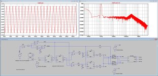
I finally got the model working properly.
A large number of blocks from a DSD256 .dsf file where skipped, and there it was the 1Khz@0dB signal in the left channel.
16 blocks split in 8 blocks Left and 8 blocks Right containing just silence, were concatenated and bytes reversed.
These 8 blocks played back over the model hold 23,216msec on information, but the sim takes almost 50 minutes to complete.
See first attachment with the result, a clean looking 1Khz sinewave together with a Blackman-Harris windowed FFT.
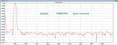
Second attachment shows the spectrum when zooming into the range up to 10Khz with no obvious distortion products.
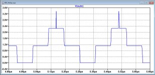
But, at this high DSD256 frequency of ca. 11.3 Mhz and using a timestep of 10nsec, I still noticed spikes coming from the Firdac after the 8 summation resistors but with no further loading, see third attachment, so in fact the 10nsec timestep is still too large.
At 1nsec timestep all spikes are gone, but at the cost of an even longer sim time, but not used for this first run.
I'll switch now to DSD64 where the contribution of eventual spikes to the spectrum will be accordingly smaller and I will also try to get an even more accurate spectrum with a smaller timestep.
There I will also try to investigate in more detail the effect of reversing bytes or leaving them as they are positioned in the .dsf file.
To be continued, step by step
Hans
A large number of blocks from a DSD256 .dsf file where skipped, and there it was the 1Khz@0dB signal in the left channel.
16 blocks split in 8 blocks Left and 8 blocks Right containing just silence, were concatenated and bytes reversed.
These 8 blocks played back over the model hold 23,216msec on information, but the sim takes almost 50 minutes to complete.
See first attachment with the result, a clean looking 1Khz sinewave together with a Blackman-Harris windowed FFT.
Second attachment shows the spectrum when zooming into the range up to 10Khz with no obvious distortion products.
But, at this high DSD256 frequency of ca. 11.3 Mhz and using a timestep of 10nsec, I still noticed spikes coming from the Firdac after the 8 summation resistors but with no further loading, see third attachment, so in fact the 10nsec timestep is still too large.
At 1nsec timestep all spikes are gone, but at the cost of an even longer sim time, but not used for this first run.
I'll switch now to DSD64 where the contribution of eventual spikes to the spectrum will be accordingly smaller and I will also try to get an even more accurate spectrum with a smaller timestep.
There I will also try to investigate in more detail the effect of reversing bytes or leaving them as they are positioned in the .dsf file.
To be continued, step by step
Hans
Attachments
I'm used to run times between 8 hours and a week on a server for sigma-delta simulations, so 50 minutes on a PC isn't bad. The time steps are usually a few dozen picoseconds, but maybe you can get away with 100 ps or so because of the slower technology, assuming you realistically model the transition times.
@ThorstenL & MarcelvdG
As I understand it the number of tabs control the stopband attenuation and the steepness of the filter
Number of taps and weights, it's complex.
and the clk frequency needs to be at least the bit rate clk or a multiplum of this. So in a non RTZ at least the DSD bit clk and preferably (?) a higher MCK.
In an NRZ (Non Return to Zero) FIR DAC we usually find DAC-CLK = BCK
In an RTZ (Return To Zero) FIR DAC we require DAC-CLK >= 2 * BCK
While in principle a higher clock is desirable, we require a situation where the rise and fall times are a small compared to the clock cycle.
I personally usually use IC DAC's, but the DSD17XX (e.g. DSD1792) from TI use an 8-Tap, unequal weight RTZ FIR DAC when playing DSD (but not PCM).
These can be in practice be used with up to 50MHz MCK and DSD1024. However when operating faster than DSD256 the SNR and HD get worse, just barely noticeable with DSD512 but very appreciable with DSD1024.
So clock speed is a compromise between multiple factors. There is no simple answer.
But what determines the cutoff and stopband frequency? The resistor values and the capacitor at the summing point? I just need the math for a equally weighted FIR filter.
DSP FIR-filter calculator, V2400
Personally I use this tool (and others, specifically https://fiiir.com/) to calculate FIR filters. But these are to calculate filters, not to go backwards from an existing filter.
By the way I saw that the SN74LV595ANSR can be operated at 5V and has a fmax of 115 Mhz, so I would guess, this could be a good candidate as an alternative to the 74FF shift register?
Ok, let's look at this in detail. First the internal diagram:
We can see we have two sets of Flip-Flop's in series. That is one more than necessary. And we have tri-state outputs.
As remarked - with correct timing we can use the two separate registers to our advantage, however I have not seen a FIR DAC design using this. So we get two sets of Flip-Flop's triggering at the same time making the device more noisy than necessary and as there is only a sole GND & PSU pin this is going to cause trouble.
At 115MHz you are very seriously pushing the timing at 5V Supply. Reliable operation past 50MHz is probably going to be hard to achieve.
One improvement could be to use 74LVC8T595, which has two power supply domains, one for all the Logic and one for the output switches.
Now any logic switching does not directly feed into the analogue reference power, but the IC is obscure and excess logic up front still causes what Ed Meither defined as "Logic Induced Modulation" affecting clock jitter inside the IC and possibly outside, depending on the competence of the PCB design.
Another issue is that all flip flop's in the 595 are internally committed into a shift register with 8 Bit's.
This was no issue for Jussi's original DAC which was single-ended, however FIR DAC's do improve if operated balanced. Now the balance at higher frequencies (above audio) will very much depend on PCB layout and it impossible to be symmetrical.
If instead using 74LVC574 we gain a number of advantages:
The Logic is more simple (less noise) and the Flip Flop are uncommitted, so we can make two 4-bit FIR DAC (sections) that are balanced on one IC.
Even some of the root causes of LIM are resolved. As we get the same number of L>H and H>L transitions in each "sample" the power spikes charging/discharging the CMOS gates in theory net off and are contained on chip.
Even better would be if there was a 74LVC8T574 version where the power for the output Buffer would be on separate pins.
We could of course use a bunch of buffers (74LVCU04?) to separate the power supply domains of logic and actual DAC.
It is noteworthy that 16 Bit D-Latches optimised for high speed bus systems operating at 1.8V or 2.5V do exist and could be used to make a single chip balanced 8-Tap FIR, like used by Electrart Japan for the so-called DSD-Principle DAC (resistor values and schematic in the Link).
The 16 Bit parts also have (IMNSHO) much better pin layout for ground and PSU, allowing much lower noise PCB Layouts than the 8-Bit parts.
So in my view, using for example SN74LVC16374A to make balanced FIR DAC's is a much better choice than either 574 or 595.
LVC or equivalent logic is especially recommended for NRZ FIR DAC, as LVC have nominally identical rise and fall time. This is unlikely to be precise, but LVC logic will reduce ISI, which manifests itself has high levels of H2 and even harmonics in a single ended FIR DAC and as increased H3 and odd order harmonics in balanced FIR DAC's.
Resist the human predilection for symmetry and always the two adjacent pins for p & n of one bit, instead of using each bank separately in a nice symmetrical picture on the screen.
Finally my "obligatory" DSD1700 reference. This was BB Japan's DAC Chip for DSD, basically designed for Sony et al.:
I think a discrete implementation of this with 2 X 74LVC16374 as shift registers, Kaiser Window weighted (or just electart's values) and RTZ with 75% duty cycle (MCK = 4 * BCK and additional logic) based on Marcel's design could produce a DAC with similar complexity and improved performance.
Equally a Jussi/Pavel DSC2 build correctly using 74LVC16374 would likely outperform this thing:
L7 Audiolab Measurements of VEZZOSO DSD-NB Discrete Δ-Σ D/A Converter
Which one would be better, discrete DSD1700 or DSD2 with 74LVC16374.... Answers on a postcard.
Thor
You can use any wave editor to draw the samples and then use FFT function, or use REW with impulse response text import (which needs to obey to the following format).But what determines the cutoff and stopband frequency? The resistor values and the capacitor at the summing point? I just need the math for a equally weighted FIR filter.
Example for 8 equal weight taps:
Code:
* Impulse Response data saved by REW V5.31 (required)
0.0 // Peak value before normalisation, don't care
0 // Peak index, don't care
1024 // Response length, defines low frequency display limit
1.0E-5 // Sample interval (seconds), make sure the sample rate is neither too high nor too low to display
0.0 // Start time (seconds) , don't care
* Data start
1.0
1.0
1.0
1.0
1.0
1.0
1.0
1.0After import, normalize to 0dBSPL at a low frequency.
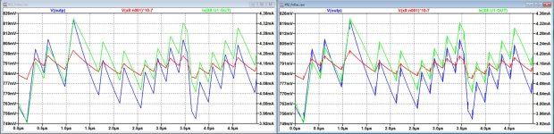
Before going into different DSD rates with even smaller timesteps, I first wanted to get a better feeling whether a more realistic 8.2nF cap as against an ideal version would make any difference.
That's why I added a 30mR series resistance and a 200pH series inductance, this according to Kemet specs for their 8.2nF NP0.
Result turns out to be rather obvious as shown in the attachment below, without at the left side and with these two series impedances at the right, where lots of spikes are visible at the moment the slope inverts its direction.
These spikes feedthrough all the way into the first OPA2210 op-amp.
Image was made with a 50psec timestep while processing the DSD256 1Khz@0dB signal.
Blue is the signal as measured on the 8n2cap.
Red is the signal on the inverting input of the OPA2210, connected with a 255R to the 8n2 cap, here for better clarity magnified by a factor 10
Green is the output current sourced by that same OPA2210 op-amp.
As such the voltage variations at the inverting input are seemingly well within range to avoid oversteering, but this is just a sim and the real thing may react different to these spikes.
@marcel, what is your view on this qua impact on the performance and could this be reason why noise becomes slightly worse when increasing the DSD rate?
Hans
P.S. I could also try Thor's filter and see what the OPA1632 makes of this 😊
Attachments
The same period as above, but now with Thor's filter, results in completely different waveforms because of the different topology.
The spikes at the point where the eight Firdac resistors enter the filter in blue, still have the spikes as before, but at the input of the OPA1632 in red all spikes are absent, but also the OPA1632's output current in green doesn't show any content of spikes just because the spikes from the Firdac's are in opposite direction and cancel each other.
This filter seems to be doing a superior job, kudos to Thor.
Hans
Attachments

Sorry to interrupt but I have a quick question regarding a possible component substitution on the DAC board. It seems that the 10ohm 1watt resistor is now out of stock everywhere with delivery in April 2025! Ouch.
These 4 are in the bases of Q30 / Q31 and the DAC ref outputs so probably quite critical as to component choice? Unfortunately due to them being relatively expensive I didn't buy spares on my previous orders.
@MarcelvdG Is there an equivalent resistor that would fit the design criteria that you could recommend please?
PCAN0805E10R0BST5
These 4 are in the bases of Q30 / Q31 and the DAC ref outputs so probably quite critical as to component choice? Unfortunately due to them being relatively expensive I didn't buy spares on my previous orders.
@MarcelvdG Is there an equivalent resistor that would fit the design criteria that you could recommend please?
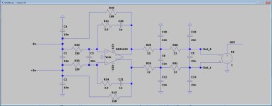
This is the one I used.Which filter do you mean?
Not yet optimised to have a perfectly flat response up to 80Khz, but representative enough to see it's behavior in the test I did.
Hans
Attachments
Would these be suitable substitute:
TNPW080510R0BEEN
The note on the circuit diagram says 200mW and these are 200mW.
Many thanks!
TNPW080510R0BEEN
The note on the circuit diagram says 200mW and these are 200mW.
Many thanks!
This is the one I used.
Not yet optimised to have a perfectly flat response up to 80Khz, but representative enough to see it's behavior in the test I did.
Hans
How did you model the parasitics of the capacitors, resistors and IC package?
Would these be suitable substitute:
TNPW080510R0BEEN
The note on the circuit diagram says 200mW and these are 200mW.
Many thanks!
Those should work fine.
- Home
- Source & Line
- Digital Line Level
- Return-to-zero shift register FIRDAC