The converters used were multiple IC's all with 8-Tap FIR filters using non-equal weights and current output, internally using DEM of 64 total unitary weight switched bit's, dynamically mapped to and 8 Bit FIR.
If we can call it DSD2048 or what to call it an interesting question for marketing people.
As the highest DSD SR commercially recorded is DSD256 (exceedingly rare), any "DSD2048" content would be upconverted from PCM or DSD64/128/256.
The object of using a high DSD sample rate in this case, specifically with PCM is to have greater actual physical resolution from the converter as a single DSD512 one would be capable of and the ability to use less aggressive noise shaping as result, while providing the same or greater noise free bandwidth as a single DSD512 DAC is capable of delivering.
By running four DSD512 systems in parallel time-shifted we get an observed ripple residue and steps in the slope of the signal that match what we would see from DSD2048, though it is created by interleaving DSD512 converters (not in the same precise way as I suggested elsewhere specific to your DAC design I might add - interleaving lacks a sufficiently narrow definition).
Conceptually this (left had side):

What was tested included RTZ at 75% duty cycle in the DAC Hardware, thus based on definitions in extant literature "increase the sample rate N-fold by using N DAC's" and thus at least under these definitions would qualify as DSD2048.
But ultimately this is all semantics.
Later testing found that in practice audible and measurable differences between a complex algorithm and a simple delay chain were very inconclusive. Improvements for both versions "Interleaved multi-DAC" solution were observed, compared to just operating four DAC's in parallel. The same situation was observed with two DAC's to a lesser degree.
Thus my personal takeaways was that what Accuphase calls "MDSD" is worthwhile to implement and relatively trivial in difficulty (especially if we use an FPGA for PCM/DSD to DSDn conversion) if we use multiple DAC's.

A number of happenings mean that it has been a few years in which I have not progressed this design. Reading about your DAC gave me impetus to resume work.
Incidentally, Accuphase also have an improvement option for the I/U conversion:

I have used similar circuits in other applications that needed low noise where it was non-trivial to achieve without major re-designs.
Thor
If we can call it DSD2048 or what to call it an interesting question for marketing people.
As the highest DSD SR commercially recorded is DSD256 (exceedingly rare), any "DSD2048" content would be upconverted from PCM or DSD64/128/256.
The object of using a high DSD sample rate in this case, specifically with PCM is to have greater actual physical resolution from the converter as a single DSD512 one would be capable of and the ability to use less aggressive noise shaping as result, while providing the same or greater noise free bandwidth as a single DSD512 DAC is capable of delivering.
By running four DSD512 systems in parallel time-shifted we get an observed ripple residue and steps in the slope of the signal that match what we would see from DSD2048, though it is created by interleaving DSD512 converters (not in the same precise way as I suggested elsewhere specific to your DAC design I might add - interleaving lacks a sufficiently narrow definition).
Conceptually this (left had side):
The concept using an analog power combiner in order to sum signals of multiple DACs is shown in Fig. 2 on the left side. The signals of the individual DACs are exposed to a phase shift relative to each other in order to guarantee a correct summation.
Furthermore, one can distinguish between two techniques as shown in Fig. 2 (b): firstly, NRZ signals can be added. However, they require a digital pre-compensation algorithm to calculate
the individual sequences contributing to the combined signal. This variant is also known as pseudo-interleaving and used e.g. in the Fraunhofer HHI Arbitrary Waveform Generator (AWG) with 70 GS/s and 18 GHz bandwidth.
Secondly, return-to-zero (RZ) signals can be used, which do not require a pre-compensation algorithm, as shown in Fig. 2 (b). Hence, this technique is called true interleaving. However, the requirements on the DAC’s switching speed are increased. Both techniques increase the sample rate N-fold by using N DACs, but the bandwidth remains constant, since the combined DAC
is limited by each DAC’s sinc-roll-off in the frequency domain.
The other concept in the time domain makes use of a highspeed MUX as shown in Fig. 2 on the right side. Multiple DACs generate analog signals, which are then aggregated to a higher sample rate with a high-speed analog MUX, which switches between the input signals. In Fig. 2 (d) the
ideal MUX operation is shown for the case of two DACs. The MUX output is generated by switching between the two input signals, whereby the MUX "samples" the input signals in the center of each symbol, which is denoted by the black dotted line.
What was tested included RTZ at 75% duty cycle in the DAC Hardware, thus based on definitions in extant literature "increase the sample rate N-fold by using N DAC's" and thus at least under these definitions would qualify as DSD2048.
But ultimately this is all semantics.
Later testing found that in practice audible and measurable differences between a complex algorithm and a simple delay chain were very inconclusive. Improvements for both versions "Interleaved multi-DAC" solution were observed, compared to just operating four DAC's in parallel. The same situation was observed with two DAC's to a lesser degree.
Thus my personal takeaways was that what Accuphase calls "MDSD" is worthwhile to implement and relatively trivial in difficulty (especially if we use an FPGA for PCM/DSD to DSDn conversion) if we use multiple DAC's.
A number of happenings mean that it has been a few years in which I have not progressed this design. Reading about your DAC gave me impetus to resume work.
Incidentally, Accuphase also have an improvement option for the I/U conversion:
I have used similar circuits in other applications that needed low noise where it was non-trivial to achieve without major re-designs.
Thor
Last edited:
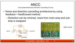
Very strange this ANCC circuit.
The I/V converter has a virtual input that should be at at the same level as the positive input, zero volt in this case.
When any deviation from zero volt takes place (apart from the tiny input voltage difference dependent on input signal and loop gain) it means that the I/V convertor isn´t fast enough to follow the input current signal.
This will be detected by a much faster Detection amp who injects canceling current.
1) Either this happens outside the BW of interest, then it protects the I-V's input from overloading by signals outside the required BW
2) When it already happens inside the BW of interest, the detection amp has no knowledge of what's noise, distortion or Audio and can only damage the signal. To prevent this from happening, the detection amp must have a high pass filter to prevent interaction in the BW of interest.
So to me it looks like an input overload protector instead of a noise and distortion canceling circuit.
Hans
It's probably simplified beyond recognition. When you simplify it a bit further by replacing the op-amps with nullors, it becomes a transimpedance amplifier with shorted input.
The I/V converter has a virtual input that should be at at the same level as the positive input, zero volt in this case.
When any deviation from zero volt takes place (apart from the tiny input voltage difference dependent on input signal and loop gain) it means that the I/V convertor isn´t fast enough to follow the input current signal.
REALLY? What an extraordinary thing to say.
So your Op-Amp has no distortion, no noise. Nothing. Infinite bandwidth while still being unity gain stable. Infinite gain too.
How extraordinary.
This will be detected by a much faster Detection amp who injects canceling current.
1) Either this happens outside the BW of interest, then it protects the I-V's input from overloading by signals outside the required BW
2) When it already happens inside the BW of interest, the detection amp has no knowledge of what's noise, distortion or Audio and can only damage the signal. To prevent this from happening, the detection amp must have a high pass filter to prevent interaction in the BW of interest.
Really? What an extraordinary thing to say.
Well, so good you already know everything and how perfect everything is, so it cannot possibly be improved upon.
So to me it looks like an input overload protector instead of a noise and distortion canceling circuit.
Sure, whatever.
Thor
It's probably simplified beyond recognition.
Not really.
When you simplify it a bit further by replacing the op-amps with nullors, it becomes a transimpedance amplifier with shorted input.
Not really. If you have a real op-amp, the voltage between positive and negative input is directly proportionate to the error on the output.
If we extract this error and inject a current that is proportionate to the error in correct phasing into the inverting node, or a voltage into the positive (normally grounded) input, what happens on the output?
See here:
https://www.tubecad.com/2004/blog0020.htm
Fun thing, I used this error correction with a bridged amplifier, where each half operated inverting.
The error extraction / cancellation circuit with injection into the other sides positive input substantially lowered the classic A/B Amp distortion products at higher frequencies.
Thor
Maybe so, for that elite group at the time. However, I've gotten lots of flack since then for advising against ferrite beads in some applications. At least Thor gets it....most of us here were in agreement about it when the issue first appeared...
The ANCC +ve input terminal with the -ve input terminal grounded? What does the arrow out of this ANCC amplifier mean?View attachment 1285551
I have used similar circuits in other applications that needed low noise where it was non-trivial to achieve without major re-designs.
"To detect and cancel the noise and distortion at the input stage of the I-V converter."
How does the ANCC network "know" what is "noise" and what is "distortion" of the current "input" signal? How does "cancelling" come into it and not potentially preventing it or "lowering" it in the subsequent I/V?
What is the nature of the "noise" being cancelled, or not otherwise amplified? Is it IM being lowered in relation to signal that the ANCC can seemingly know to differentiate?
This blurb seems hopelessly inept.
It depends who in marketing dept was responsible for the drawing.It's probably simplified beyond recognition.
This may make more sense. (page 8 in https://www.accuphase.com/technical_information/dg-68_technical_information.pdf)
Attachments

One paper attached. Be nice if Thor would be so kind as to post the Accuphase material.
The paper describes a different method, which is why I did not post a link to it. For us relevant is really just first/second page.
The ANCC +ve input terminal with the -ve input terminal grounded? What does the arrow out of this ANCC amplifier mean?
It is not a technical article or service schematic. It shows a fundamental principle and likely so you need to think a bit to spot the obvious intentional "schematic mistakes".
"To detect and cancel the noise and distortion at the input stage of the I-V converter."
How does the ANCC network "know" what is "noise" and what is "distortion" of the current "input" signal?
It doesn't "know" of course.
It can only "detect and cancel the noise and distortion at the input stage of the I-V converter.", of the I/U converter of course.
How does "cancelling" come into it and not potentially preventing it or "lowering" it in the subsequent I/V?
You extract the error and inject the error with correct phase and amplitude back into the signal circuit.
In an ideal circuit, all distortion and noise is cancelled (but then, there is no such thing in the first case).
In a real circuit the error correction Op-Amp is commonly the limit, plus, I have never been able to get such cancellation schemes much past 20dB... Then again, 20dB lower noise or HD are worth having.
What is the nature of the "noise" being cancelled, or not otherwise amplified? Is it IM being lowered in relation to signal that the ANCC can seemingly know to differentiate?
The ANCC Circuit does not actually distinguish what noise etc, it "looks" at the inverting op-amp pin and "thinks" to itself: "This should be zero, if it's not zero, what is there is a fidelity impairment that I need to action to make zero."
This blurb seems hopelessly inept.
Bad English translation from Japanese that was overly simplified.
Given that is such an utterly basic set electronic concept's involved, I did not see a need to belabour the point, it was just something noticed in passing while I was looking for the illustration of multiphase DSD.
Thor
It depends who in marketing dept was responsible for the drawing.
This may make more sense. (page 8 in https://www.accuphase.com/technical_information/dg-68_technical_information.pdf)
Yes. This is plain old error feedforward, older than Black's feedback patent.
Ha, ha, very funny, but your comment shows that you did not understand my reaction, so this is obviously not your world.REALLY? What an extraordinary thing to say.
So your Op-Amp has no distortion, no noise. Nothing. Infinite bandwidth while still being unity gain stable. Infinite gain too.
How extraordinary.
Really? What an extraordinary thing to say.
Well, so good you already know everything and how perfect everything is, so it cannot possibly be improved upon.
Sure, whatever.
Thor
Hans
Yes thx, this feedforward circuit is a proper topology.It depends who in marketing dept was responsible for the drawing.
This may make more sense. (page 8 in https://www.accuphase.com/technical_information/dg-68_technical_information.pdf)
Hans
Have you tried slowing the risetime of the clock? If not, maybe stick a physically small one-turn 200R pot in series with MCLK or BCLK just before it goes into dac (whichever one clocks the dac output). After the pot there will be some capacitance so an RC filter will be formed. Yes, it will cause reflections and it if too much resistance then the dac may not be able to work properly. But there will probably be some range over which it will still work. Adjust to pot to see what it does to the sound. Do you notice anything?My own listening on a NoDAC DSD suggests something similar regarding the (slight) thinness but why may/might it be so?
Back in the days, Wadia did experiment with adjusting series damping on I2S and clock signals. The also experiments short timed-delays (with normal rise-time) that shouldn't make any difference. They found that there were sweet spots where dac sounded better for not clearly understood reasons. I found the same with ESS and AKM dacs. Sometimes a MCLK series damping change of 5R is enough to hit or else miss the sweet spot (in one case I needed exactly 135R). When I was trying time delays in 200ps steps, one step difference could have a small effect on the sound. Again, either hit a sweet spot or miss it.
Last edited:
Thx Mark.One paper attached. Be nice if Thor would be so kind as to post the Accuphase material.
Referring to this source was clearly an omission in Thor’s posting.
Hans
I think the ANCC circuit in post #2441 is supposed to have a finite transconductance that is close to the reciprocal of the feedback resistance of the transimpedance amplifier (current-to-voltage converter). It then acts as a negative resistance equal to the opposite of the feedback resistance of the transimpedance amplifier. The gain from the error voltage of the transimpedance amplifier's op-amp to the output is ideally the sum of the two resistances divided by the ANCC resistance, so (-R + R)/(-R) = 0.
The amplifier in the ANCC circuit is drawn as an op-amp, so I originally thought that the circuit was supposed to behave ideally when its gains approach infinity, which made no sense.
The amplifier in the ANCC circuit is drawn as an op-amp, so I originally thought that the circuit was supposed to behave ideally when its gains approach infinity, which made no sense.
Marcel,
Yes indeed, that creates a working solution, but it could be a delicate exercise to match those resistances over de required BW.
On the other hand, with modern op-amps having two digit Mhz GBW's with THD's in the ppm, what's the sense of using this complex solution ?
Hans
Yes indeed, that creates a working solution, but it could be a delicate exercise to match those resistances over de required BW.
On the other hand, with modern op-amps having two digit Mhz GBW's with THD's in the ppm, what's the sense of using this complex solution ?
Hans
Sure Marcel... though what is the point? The signal input is still connected directly to the inverting input of the I/V. What does creating this seeming impedance shunt to ground do... unless being of some dynamic shunt to divert high frequency currents from the I/V input. This also requires considerable care not to create more problems than benefits. Stability being an issue as the ANNC network is also part of the feedback path.
Yes indeed, that creates a working solution, but it could be a delicate exercise to match those resistances over de required BW.
That probably explains why Thorsten only got 20 dB of improvement.
@Markw4 : Thanks for your feedback ...
Yes, I have. I mounted some of the TX-42 mini-trimmers in place of the series resistors, however, in those days the NoDACs I used didn't perform as well THD-wise as the current ones do, so I couldn't see any difference on the output (I only measured the output signal).
With the recent NoDACs I have tried to replace the resistor that was optimum relative to low (no) reflections with a 100 ohm resistor and it didn't change the distortion spectrum (almost) at all - except for a very tiny difference in the skirt height of the fundamental tone. It made me think of something bohrok2610 had mentioned in this thread:
https://www.diyaudio.com/community/threads/measuring-phase-jitter.406540/page-3#post-7542344
As it is the optimum resistor had the lowest skirt height whereas the 100 ohm resistor displayed a slightly higher skirt level. I reckon it would indicate that the 100 ohm resistor caused more close-in phase noise in the circuitry - possibly also altering the sound? The latter I don't know about by now as I haven't listened to it yet ...
Cheers, Jesper
Have you tried slowing the risetime of the clock?
Yes, I have. I mounted some of the TX-42 mini-trimmers in place of the series resistors, however, in those days the NoDACs I used didn't perform as well THD-wise as the current ones do, so I couldn't see any difference on the output (I only measured the output signal).
With the recent NoDACs I have tried to replace the resistor that was optimum relative to low (no) reflections with a 100 ohm resistor and it didn't change the distortion spectrum (almost) at all - except for a very tiny difference in the skirt height of the fundamental tone. It made me think of something bohrok2610 had mentioned in this thread:
https://www.diyaudio.com/community/threads/measuring-phase-jitter.406540/page-3#post-7542344
As it is the optimum resistor had the lowest skirt height whereas the 100 ohm resistor displayed a slightly higher skirt level. I reckon it would indicate that the 100 ohm resistor caused more close-in phase noise in the circuitry - possibly also altering the sound? The latter I don't know about by now as I haven't listened to it yet ...
Cheers, Jesper
- Home
- Source & Line
- Digital Line Level
- Return-to-zero shift register FIRDAC