Hi Steph1777 i just discover this project, where i can find your last pcb ?
Thanks for sharing cool projects
Hello,
The project is not finished. I should receive the first batch of prototype PCBs at the beginning of next week. You can also follow the project on the French "Forum Bleu" or on Github.
Stef.

Hello,
I am still trying to report a little bit what I take from the simulation models of the Q17.
One important point is the error correction by the current damping bridge, which works extremely precisely with the Q17, much more precisely than with usual amplifiers. This is a finding and an essential point that makes this amplifier special.
Another insight comes from the simulation for sources resistors of the output transistors. If you change the value from a few mOhm step by step up to 1 Ohm, you can see at about 0.3 Ohm that the amplifier starts to produce deformations of the signal and the error correction obviously does not work properly anymore. I came across this because the peaks to compensate for the capacitances of the Mosfet become larger even at small source resistances.
Finally, it explains that the Q17 with two pairs of output transistors without sources resistors played as expected. The first amplifier with 3 pairs of outputs and 100 mOhm source resistors each also made less interfering noise than the last one with 150 mOhm resistors.
Therefore, I can give the advice to use source resistors smaller than 100 mOhm if possible in the actual builds with multiple pairs of output transistors.
Regards Tim
A non inductive resistor will be best here (R26 R27 R28).
Mills Resistor 560R Ohm 5W MRA-5 Series
Regards,
Tibi
Hello Tibi!
Just to tell you that I finally managed to find the place on the PCB to fit 3 Dale 1W resistors for the bridge.
Stef.
Attachments

Hello,
I'm thinking about a version of the PCB I'm working on with input capacitor for DC protection.
To save space, I replace the large capacitor of 1uF MKP10 by a Wima MKP2 1uF 63v capacitor (L7.2 W5.0 H10.0 P5.0). I can then use the space recovered to put an input capacitor there.
What would be the necessary value either using an electrolytic capacitor (polarized or BP) or using an MKP2 film capacitor?
A perverse effect of replacing the Wima MKP10 with a Wima MKP2 is that the MKP2s are much harder to source.
Stef.
.
Attachments
Last edited:
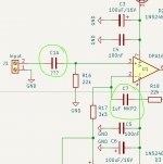
I'd say this is a 1st order high-pass filter whose -3 dB cut frequency is 1÷(2×pi×R16×C1A). Then 1µF would give ~7Hz.
This is my first post on this thread that I regularly read as I like the idea of a re-engineered 405 very much, looking for a proper amp to drive my newly hosted Kef 107... I've just registered on the Forum Bleu you've mentioned.
This is my first post on this thread that I regularly read as I like the idea of a re-engineered 405 very much, looking for a proper amp to drive my newly hosted Kef 107... I've just registered on the Forum Bleu you've mentioned.
Hello!
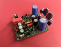
I did a test with a D10mm electrolytic capacitor input (CA1) and MKP2 film capacitor for C7 with a footprint that can accept capacitors with 5mm, 7.5mm and 15mm pitch. Nothing more can be brought in. It is therefore either MKP2 or MKT / MKS film capacitors.
If we replace the input capacitor CA1 by an MKP2 film, we can place a 5mm / 7.5mm pitch footprint for each of the capacitors, or maybe C7 with 15mm too. Should try.
Not easy to choose.
In the photo, the "small" red capacitor is the place that the Wima MKP2 would occupy.
Stef.
.
Attachments
Last edited:
Hello!
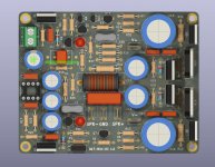
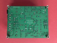
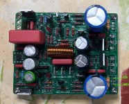
The first prototype of the Q17-Mini is assembled. 🙂
All that's left for me to do is mount it on a heatsink and plug it in. I keep my fingers crossed so there is no mistake.
The continuation soon.
Stef.
.
The first prototype of the Q17-Mini is assembled. 🙂
All that's left for me to do is mount it on a heatsink and plug it in. I keep my fingers crossed so there is no mistake.
The continuation soon.
Stef.
.
Attachments
Last edited:


Take care !
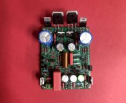
Before you start testing your nice creation, please take a look at all you solder joints ! You missed at least one in the groundplane!
Good looking PCB, Good luck !
Before you start testing your nice creation, please take a look at all you solder joints ! You missed at least one in the groundplane!
Good looking PCB, Good luck !
Before you start testing your nice creation, please take a look at all you solder joints ! You missed at least one in the groundplane!
Good looking PCB, Good luck !
Thank you. I hadn't seen that one.
Stef.
Hello!
No chance. It does not work.
When I plugged in the board (48vDC), the meter displayed a consumption of 400W (at main 230V) and -1.5v DC at the HP output (without 8R charge). I cut off the power after a few seconds. No burning smell, no capacitor explosion. I have no short circuit between the transistors through the heatsink.
I'm good at checking everything. 😡
Stef.
Hello!
Again me.
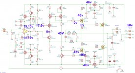
I removed the power transistors (Q5, Q6, Q15 and Q16). No more delusional consumption. BUT I found 43v on pin 1 of Q6. It doesn't seem right. I removed Q12 to be sure. Always 43V.
I don't see where it came from. I don't see any solder short circuit at the moment.
Supply is +-50VDC at input of the board.
If someone has an idea?
Stef.
Again me.
I removed the power transistors (Q5, Q6, Q15 and Q16). No more delusional consumption. BUT I found 43v on pin 1 of Q6. It doesn't seem right. I removed Q12 to be sure. Always 43V.
I don't see where it came from. I don't see any solder short circuit at the moment.
Supply is +-50VDC at input of the board.
If someone has an idea?
Stef.
Attachments
Last edited:
...
If someone has an idea?
Stef.
Use a soft start, or a bulb as Vrystaat mentioned.
-43V on gate of Q6 is ok.
Rail voltages after Q13 and Q14 should be +/-46V.
Measure voltage after regulators, should be around +/-14V.
Voltage across R3, should be 0,6V.
Solder back Q5 and Q6. These will get hot quickly. See if voltage across R11 and R12 is ~3V on each and ~+/-3V relatively to ground.
Solder output transistors and measure output dc, should be under 1mV.
Regards,
Tibi
Correction !!!
It is normal to have +43V on gate of Q6 as you have removed Q6.
There is no base current on Q12, therefore this is open and is normal to see positive rail Q6 pin 1.
Regards,
Tibi
It is normal to have +43V on gate of Q6 as you have removed Q6.
There is no base current on Q12, therefore this is open and is normal to see positive rail Q6 pin 1.
Regards,
Tibi
Last edited by a moderator:
Solder back transistors and measure output. If this under 1mV dc, amplifier should work.
Regards,
Tibi
Regards,
Tibi
Hi!
Im' using a Connex SMPS... 😡
A mesured some voltages (without power transistors).
A also tried with Q5 and Q6 (without Q14 and Q15). R8 smoked in 15 secondes.
Stef.
.
Im' using a Connex SMPS... 😡
A mesured some voltages (without power transistors).
A also tried with Q5 and Q6 (without Q14 and Q15). R8 smoked in 15 secondes.
Stef.
.
Attachments
Last edited:
- Home
- Amplifiers
- Solid State
- Q17 - an audiophile approach to perfect sound