Hello!
Does an "official" Q17 diagram with more than a pair of power MOSFETs exist?
Stef.
Q17 - a QUAD405 audiophile approach to perfect sound
Please note that this triple pair was not constructed or tested by me.
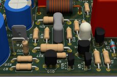
So far this amplifier was tested with a single pair vertical mosfet, double pair vertical mosfet, double pair exicon lateral mosfet and quadruple pair exicon double die lateral mosfet at +/-85V.
Regards,
Tibi
Last edited by a moderator:
Tanks Tibi,
Quad pair at 85v !! Don't fit on my PCB 😉
With a single pair and Exicon, do we need to add components and/or change values of some?
I just finished checking all the resistances of the proto PCB. It's not fun to do but I found several footprints too small or with holes too big. Difficulty finding the place but done. The famous R32 is standing now. 😉
Stef.
Attachments
Last edited:
Hello Tibi,
I will take your advice into my designs and of course I will check what the simulation says. I know that simulations are never correct, but I come from a younger generation and therefore I solve many technical questions with approximate solutions and less with analytical equations. I have had very good experience with this in my loudspeaker development.
Another point is the capacitors for voltage stabilisation of the opamps. Here I can say from experience in optimising DAC and headphone amplifier that PS films are not the sonic end. For the Q17, I had already considered 100nF MKP10, which has a pitch of 10mm, so it is also considerably larger. The FKP2s I have installed are a dream in relation to sound, price and size. However, with the restriction that they are only available up to 33nF. Therefore, in my layout for the Q17, which incorporates all the experience I have gained, I have now entered both for the current stabilisation of the OPA.
Regards Tim
Attachments
...
With a single pair and Exicon, do we need to add components and/or change values of some?
...
You are welcome !
For Exicon, or other laterals, you need to change gate resistors - as I mentioned in my previous post - and R11 = R12 = 10ohm.
Regards,
Tibi
Tim,
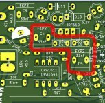
I would suggest you to move decoupling 33nF capacitors as close as possible to opamp.
I think your intention, with R22 and C27, was to limit amplifier BW, but in fact you created a new Fc pole where the amplifier gain will increase, because R6 is part of negative feedback together with R27.
A better solution would be to use an inductor in series with R6=100.
Some fast calculation: for Fc =1MHz L=R/(2PIxFc)=100/(2x3.1415x1000000)=16uH
This will create a pole at 1MHz where amplifier gain decrease.
Regards,
Tibi
Last edited by a moderator:
Hello Tibi,
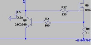
either my LTspice model is completely wrong, or there is some unusual behaviour in the system that could be eliminated with a capacitor + resistor (2,2nF+10Ohm) on the collector of Q12. Can you please check this in your simulation model?
I am comparing the frequency responses of gate Q5 and gate Q6.
Regards Tim
Attachments
Last edited:
Hello Tibi,
The post 507 was not a good idea. I notice that the simulation breaks down / becomes unstable when I add Source resistors to FQA36P15. I am currently experimenting with a drain resistor of Q6, that helps the most. The two capacitors in my setup act similarly as a load for the class A amplifier, so that makes it stable too - says the simulation.
I cannot consider a reduction of R10 and R13 as favourable after the simulation.
Regards Tim
Hello Tibi!
Short question for you. For R27 in the bridge, you used an Ohmite 560R carbon 1W resistor.
Is it intended to use carbon there?
I ask because it is big this kind of resistance and the place is counted on my PCB.
Stef.
Short question for you. For R27 in the bridge, you used an Ohmite 560R carbon 1W resistor.
Is it intended to use carbon there?
I ask because it is big this kind of resistance and the place is counted on my PCB.
Stef.
A non inductive resistor will be best here (R26 R27 R28).
Mills Resistor 560R Ohm 5W MRA-5 Series
Regards,
Tibi
Mills Resistor 560R Ohm 5W MRA-5 Series
Regards,
Tibi
A non inductive resistor will be best here (R26 R27 R28).
Mills Resistor 560R Ohm 5W MRA-5 Series
Regards,
Tibi
5W ???
I already don't have much space but a 5W ...
Stef.
ok. 😉
Times are tough. The DALE 1W some is the series (CPF, ALSR, etc.) are sold out for 560R and I do not have a 560R Dale in stock.
I was planning to put a sorted Vishay PR01 in the meantime. The Ohmite carbon is definitely too big for the PCB.
Stef.
Times are tough. The DALE 1W some is the series (CPF, ALSR, etc.) are sold out for 560R and I do not have a 560R Dale in stock.
I was planning to put a sorted Vishay PR01 in the meantime. The Ohmite carbon is definitely too big for the PCB.
Stef.
A failed experiment:
i tried to understand the simulation of the Q17 with LTspice more closely. I have a model in which the FQA and FQP MosFET are placed. Thereby I have the gate voltages displayed. When the driver stage has a small offset, the gate voltages become more similar in level. According to my understanding the class A driver stage works very unbalanced. Therefore an experiment:
At R13 = 8.35 ohms, the DC offset in the simulation drops below 1mV. R10 remains unchanged at 10 ohms. Therefore I soldered at R13 to the 10 Ohm resistor a 47 Ohm resistor (approx. 8.3 Ohm) to listen in reality how the amplifier plays. The special: it does not play. But he has pulled the 600W of the transformer (only one module), because the fuse of the transformer with 3,15A (at 230V) has tripped. After rebuilding it doesn't play either, but I didn't take the time to find out which components were destroyed. I assume it was just the small transistors oscillating at very high levels in the high frequency range.
I find the experiment very interesting because I created only a small asymmetry in the structure, and the amplifier destroys itself.
This was now the 3rd Q17 that has broken while making slight modifications.
Therefore, be careful, prudent and sensitive to the Q17, it is a work of art when it performs to its full potential and a mimosa when you try to modify it.
Regards Tim
Therefore, be careful, prudent and sensitive to the Q17, it is a work of art when it performs to its full potential and a mimosa when you try to modify it.
Surely the topology of the printed circuit board is not the last influence.
...Therefore I soldered at R13 to the 10 Ohm resistor a 47 Ohm resistor (approx. 8.3 Ohm) to listen in reality how the amplifier plays. The special: it does not play. But he has pulled the 600W of the transformer (only one module), because the fuse of the transformer with 3,15A (at 230V) has tripped. ...
Can you please measure again your 47ohm resistor ? What you describe may happen with a 4,7ohm one.
Regards,
Tibi
Hello Tibi,
I had not looked closely at the simulation. This gives 360° offset for the design with R13 = 8.35 ohms for the electrical phase. This is of course an indication that the iteration gives nonsense output, or that the time offset is a problem. Or in other words: the 360° offset of the simulated phase indicates a mathematical problem of the simulation.
Now to a solution suggestion for the variant with three end transistor pairs:
R11 + R12 = 56 Ohm
R26 + R28 = 33 Ohm
R27 = 806 Ohm
C10 = 68 pF
L1 = 1.7 uH
The goal is to increase the gate voltage of the output transistors. This undoubtedly results in an increased quiescent current, but the operating point and the associated problem should become more balanced.
What do you think about this?
Or would you only want to agree to increase R11 + R12 = 51 ohms, as a possible optimization?
Last edited:
I do not understand what you mean by "360° offset for the design".
Can you share your schematic, please ?
Decreasing R13 will increase class A stage current (lets name it Iq), formed with Q5 and Q6. This have direct implication on output stage as well, as the bias for output transistors increase as well R11 x Iq and R12 x Iq. Amplifier may no longer operate in class B and, depending on your R13 value, will jump more or less in A/B class.
If R13 is too low, than voltage across R11 and R12 will open Q15 and Q16 completely. These Fairchild are serious transistors, able to surge over 60 Amperes. This is what I think happened in your test, but not at R13=8,35 ohms.
If you reduce R13 you need also to "balance" Vgs on output transistors by reducing R11 and R12 and keep Q15 and Q16 Vgs around 3.1V ~ 3.2V.
If you want to change current dumping bridge, than you must take care on R6 as well, because together with R27 these form amplifier negative reaction.
Regards,
Tibi
- Home
- Amplifiers
- Solid State
- Q17 - an audiophile approach to perfect sound