PN4391
Good news about PN4391.
I bought some from Futurlec: PN4391 - PN4391 N-Channel Switch Transistor .
I sent one to Marko (stormsonic) who compared it with curve tester (or plotter) to his MMBF4391's and it is genuine.
Thank you, Marko.
Good news about PN4391.
I bought some from Futurlec: PN4391 - PN4391 N-Channel Switch Transistor .
I sent one to Marko (stormsonic) who compared it with curve tester (or plotter) to his MMBF4391's and it is genuine.
Thank you, Marko.
Joshua, do you plan on matching any of them?
If so, what method are you going to use?
Thanks...
If so, what method are you going to use?
Thanks...
I'm going to match them by Vgs at the operating Id, either in the actual circuit or in a test gig with CCS set to the proper Id.
@Andrew
An ignorant question: what's happen with JFET's with higher Idss than 9,2mA?
An ignorant question: what's happen with JFET's with higher Idss than 9,2mA?
Last edited:
Look at the plots.
Extrapolate to what you think the new curves should roughly be for higher value Idss devices.
eg.
a 12mA Idss device when plotted on the Id vs Vgs graph will cross the 0Vgs axis at 12mA
The initial slope will be roughly parallel to all the others.
It will curve round similar to all the others.
It will cross the ~0mA axis at a high Vgs voltage.
There is a formula given by Borbely and others, that relates Vp to Idss and gm.
There are also formula that relates Vgs to Id, when the other parameters are known.
ID = IDSS * [1 - (VGS/VP)]2
gm = |2 * (IDSS/VP) * [1 - (VGS/VP)]|
VGS = VP + 0.63V
VGS = VP * [1 - sqrt(ID/IDSS)]
gm = |2 * (IDSS/VP) * [1 - (VGS/VP)]|
VGS = VP + 0.63V
VGS = VP * [1 - sqrt(ID/IDSS)]
Last edited:
I'm going to match them by Vgs at the operating Id, either in the actual circuit or in a test gig with CCS set to the proper Id.
That's what Andrew instructed me to do...build a test jig using the same value resistors and voltage as the circuit.
I find when measuring the J107 and a few PN4391s, the Vgs measurements can have a pretty wide spread.
Vgs + 0.63V is an estimate.
The 0.63V was extracted from the graph.
It applies to the device that Borbeely was discussing in that paragraph.
Other devices will be different, some very different.
The 0.63V was extracted from the graph.
It applies to the device that Borbeely was discussing in that paragraph.
Other devices will be different, some very different.
The Vgs at a particular Id will vary with Idss and gm.That's what Andrew instructed me to do...build a test jig using the same value resistors and voltage as the circuit.
I find when measuring the J107 and a few PN4391s, the Vgs measurements can have a pretty wide spread.
That combination of parameters are all over the place with FETs.
That is why the Vgs appears all over the place.
But once you have >2*Vp across each device, small differences in the applied voltage does not make much difference.
i.e. the device parameters become less significant when the device is operated inside it's "good operating window".
And for this particular circuit, cascoded CCS or follower, Borbely's rule is important.
It's the same for all active stages.
You choose the operating conditions to eliminate dependence on device parameters and then feedback controls the major performance targets.
Matching JFETs for Calvin Buffer
Since I was asked in a PM about matching JFETs, I'd rather detail here the method I have in mind so that all can see it and comment about it, if there may be a mistake on my part, or if there is a better way to do it.
I'm going to use a Test Jig like in the attached schematics.
(Instead of the DC current meter, a 100 Ohm resistor can be placed and the Idss current will be derived from measuring the voltage across it).
Initially position 2, 3 and 4 of the rotary switch, as in the schematics, are going to be unoccupied, or not connected.
First step:
I'm going to select pairs of master JFETs matched by both Idss and Vp. (In my case the master JFETs are 2SK170, in other cases they may be PF5102 or LSK389).
For measuring Idss the momentary switch in the attached schematics will be pushed.
For measuring Vp the rotary switch in the attached schematics will be in position 1.
Matching the Idss of the master JFETs is most critical.
Second step:
In position 2 of the rotary switch I'll place one of the selected master JFETs and instead of the 500 Ohm trimmer I'm going to wire the actual source resistor that will be used in the circuit, which is 2.2 Ohm.
In the position of the DUT I'll select pairs of slave JFETs matched by Vgs (in my case PN4391, in other cases they may be J107 or SST4391).
For measuring Vgs the rotary switch in the attached schematics will be in position 2.
Attachments
selecting the Master by Idss and Vp should work well.
I have not used the Vp, but since it is part that defines gm then it is a good way to get a matched pair.
Selecting by Idss alone is not as good.
Selecting Slave by Vgs at the actual circuit operating current is a good method.
Your jig and method will work well.
I have not used the Vp, but since it is part that defines gm then it is a good way to get a matched pair.
Selecting by Idss alone is not as good.
Selecting Slave by Vgs at the actual circuit operating current is a good method.
Your jig and method will work well.
So using the circuit below that Andrew suggested isn't any good for matching the "master" JFETs?
Then will it work for matching the "slave" devices by measuring their Vgs while using one of a matched pair(by Idss using some other method) of "master" devices?
Then will it work for matching the "slave" devices by measuring their Vgs while using one of a matched pair(by Idss using some other method) of "master" devices?
Attachments

So using the circuit below that Andrew suggested isn't any good for matching the "master" JFETs?
…
The circuit you posted is a partial circuit. Where is the -15V?
I cannot relate to a partial circuit.
Should you build the entire buffer circuit and have there a socket so that you'll be able to swap one of the slave JFETs, you'll be able to measure the Vgs of the JFET and match slaves for Vgs.
The circuit you posted is a partial circuit. Where is the -15V?
I cannot relate to a partial circuit.
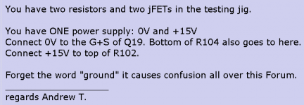
Joshua, if you'll look back at posts #314 and #315, Andrew doesn't say anything about needing -15V to measure the Vgs of the "slave" FETs.
In fact, I'll save you the trouble of going back by posting what he stated in the attachment below.
Personally...I've found the method of measuring Idss, by measuring the voltage drop across a 100 ohm resistor in series with the drain(like in the Forssell jig you posted), gives somewhat inconsistent and varying voltage readings...especially with higher Idss FETs where the FET heats up quickly.
Perhaps if you're "quick on the draw" as to reading the voltage before the FET heats up too much, you'll get a pretty good estimate of Idss.
Perhaps Andrew or Calvin can chime in because at this point since I don't really know what to do as far as "matching" these transistors.🙁
Attachments
Last edited:
Ammel,
I'll let Andrew and Calvin reply the questions you asked them.
I can only repeat myself: either make the matching with a jig like the one I posted, or in the actual circuit, with the correct resistors values and voltages.
BTW, in my post #471 there was an error on my part.
When matching the slaves Vgs, the source resistor of the JFET in position 2 of the rotary switch should be higher than 2.2 Ohm, since in the actual buffer the BJTs current also pass through it.
Taking the current values in Calvin's simulation, in one circuit option there is 51.4mA flowing through the 2.2 source resistors, which is a voltage drop of 113.08mV. Since in that simulation through the JFETs flow 4.41mA, to get the same Id in the jig, the source resistor has to be about 25 Ohm (actually about 25.6 Ohm, which is probably nonexistent).
Since in my buffer the master JFETs' Idss may be different than in Calvin's simulation, I'd rather match the slave JFETs for Vgs in the actual circuit, temporarily placing a socket in place of the slave JFETs.
The -ve voltage is needed for the Vp measurement, not for the Idss measurement.The circuit you posted is a partial circuit. Where is the -15V?
I cannot relate to a partial circuit.
Should you build the entire buffer circuit and have there a socket so that you'll be able to swap one of the slave JFETs, you'll be able to measure the Vgs of the JFET and match slaves for Vgs.
If post473 sch is used as a testing jig for checking Id of the master inside the cascoding voltage of the Slave, then it works. But there is a condition.
select all your near identical Idss high gm devices into batches.
Swap between these pre-selected devices and when you find any that have the same current Id and thus the same Vds, you know that they have changed by the same amount from the Idss test. That confirms they have the same gm (slope).
Matching requires Idss and gm to be the same. It's the starting point at the Y axis and the slope from that starting point that gets one to the operating point. At the operating point we expect the Id and the Vgs and the slope all to be "matched".
There are many ways to arrive at tests that give this double (or triple) barreled result.
I have posted details of an LTP style method & jig that does it differently and it has proved exemplary in identifying very good matching over a range of Id.
Last edited:
or in the actual circuit, with the correct resistors values and voltages.
Joshua,
Since I have a PCB, I can build one complete channel of the buffer, power it with +-18V and use sockets in all 4 locations for the FETs.
If I do this, how do I match the master devices?
Thanks...
- Home
- Source & Line
- Analog Line Level
- Preamp-Buffers - simple idea