Hi,
I have two LSK389 are 8 mA, could I use jumper for R2/3?
TIA
Felipe
Though not an expert on JFETs, I doubt it, since the JFETs need some bias for proper and stable operation.
Anyhow the difference between Zout of 34.7Ohm and 41.1Ohm or 48.2Ohm isn't that big. It should make no apparent difference in normal use, for loads higher than, say, one or few Kilo-Ohm.
By what Calvin wrote on posts #1 and #22 here, it seems that in this circuit, the quality of the PSU is much more important than a difference of few Ohm in Zout.
After all the theory, it's very simple to build the circuit with source resistors and compare the performance with the option of the source resistors shorted.
Calvin some alternative easy to source for 4391? Could be BF246C?
According to post #333, J111 (available at Mouser) combines well with 2SK170. J111 are process 51 that Calvin mentioned on post #321 as generally suitable for the upper devices.
Joshua did you make any circuit?
Not yet, it will take me about a month, maybe more.

Hi,
You may of course omit with the source resistors of circuit ´A´and ´B´, but the Matching between the two JFETs requires higher precision if the output offset shall stay low.
Alternatively You may use a AC coupling cap in the output to block the DC offset.
You need to watch if the heat power losses remain acceptably low and that no runaway occurs.
The problem is excess Gate leakage.
Gate leakage is rather seldomly stated in DS as graph and if stated as a figure, the measurement conditions are totally off of praxis.
Typically You find values around 5-10nA , measured at 0V drains source voltage and @25°C.
Btw. the Fairchild DS of the J201-203/MMBFJ210-203 shows such a graph.
But gate leakage rises sharply at drain-source voltages of more than approximately 1/4 the specified maximum Vds.
For a 25V type like the BF246 this means that if it runs at more than ~6V gate leakage may become a problem.
Secondly Gate leakage rather explodes under high temperature i.e. high current conditions.
All three conditions combine with the simple JFET-Follower of circuit ´A´
If now the Gate of the JFET is loaded by a large Gate resistor (quite often 1MOhm) the gate leakage leads to a voltage drop over the Gate resistor which in turn increases the Gate-Source voltage (decreasing the mean of Vgs, remember Vgs is negative).
This in turn increases the drain current and temperature, which in turn increases Gate leakage and so on.
Eventually the JFET may run into Latch-Up and is destroyed.
The circuit ´B´is not affected, by this, because the Master JFETs Drain-source voltage is kept low by the cascoding Slave JFET.
The Slave-JFET is not affected as its gate resistor can be choosen small and its idle currrent remains way off of its maximum, the Idss.
So, the specced maximum drain-source voltage is a important device parameter here.
With typical supplies around 15-24V the JFET´s Vds(max) should be no lower than 30-40V.
How to find the right device for the cascoding Slave JFET?
Referring to circuit ´B´in #1, You see that the Gate of the cascoding J3 is connected via R7 with the source of the Master-JFET J2a.
This means that the drain-source voltageof J2a equals the gate-source voltage of J3.
We can neglect the gate leakage (current) of J3´s gate, so there´s no voltage drop over R7.
R7 is only there to prevent possible oscillation tendencies. It could even be omitted with by a shortcut.
Now J2a and J3 are connected in series towards the supply, meaning that the same idle current runs through them.
The amount of current though is defined by the Master J2a and its source resistor (as long as the gate voltage is 0V, which is due to R4 beeing connected to signal gnd).
As this current is also running through J3 its gate-source voltage automatically sets to a certain value that can be evaluated from the Datasheet graph of drain-current over gate-source voltage (Id/Vgs).
Due to the high transconductance even large variations of drain current lead to very small variations of the gate-source voltage.
This in turn means, that the Master JFET J2a works under quite constant drain-source voltage conditions, which not only kills the Miller effect in amplifiers, but also allows for very low THD values of the Master-JFET.
We need to find a Slave JFET now that ´gives´ the Master a drain-source voltage of a couple of Volts at a couple of mA drain current, say for example ~-4V and ~8mA.
In the attached Pic You find the Id overVgs simualton of a SST4391.
The Datashet specifies:
For a gate-source voltage of 0V the drain current Idss can be between 50mA and 150mA.
For a negligibly low drain current Id=10nA the gate-source voltage (Vgs(off)) may vary between -4 and -10V.
The simulation gives us: Idss= 103mA and Vgs(off)~-5.8V
Following the graph a Id of 8mA corresponds with a Vgs of -4.2V.
This way You may find the right Slave JFET.
In short: Idss of >50mA, Vgs(off) <-3V, Vds(max) >30V.
You´ll find the J107 rather low regarding Vgs(off) and Vds(max).
J108 and J109 seem better if their low Vds(max) is acceptable.
Same applies to J310.
The J175 (and to a lesser degree) J174 seem ok also.
The 4391 still remains the most promising candidate though.
jauu
Calvin
Attachments
Thanks Calvin, I have on my stash J109BL & V grade wich Idss have I to match for my LSK389 with aprox. 8mA Idss?
TIA
Felipe
TIA
Felipe
…
This way You may find the right Slave JFET.
In short: Idss of >50mA, Vgs(off) <-3V, Vds(max) >30V.
You´ll find the J107 rather low regarding Vgs(off) and Vds(max).
J108 and J109 seem better if their low Vds(max) is acceptable.
Same applies to J310.
The J175 (and to a lesser degree) J174 seem ok also.
The 4391 still remains the most promising candidate though.
…
Calvin
Hi Calvin,
Thank you.
How about J111 with Vds=-35V, Idss min 20mA, typical 50mA and Vgs(off) between -3V and -10V -- when selecting samples for desirable Idss and Vgs(off)?
Hi,
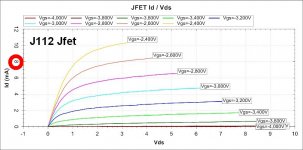
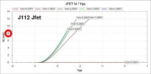
the graph in #352 is characteristic for all JFETs.
To evaluate if Your candidate is suitable for the cascoding task have a look in the datasheets and the graphs.
If the DS contains only specs but no graphs, then you can estimate the Vgs at a certain Id in a first aproximation by drawing a straight line in a Id over Vgs graph instead of the real bowed curve.
The end points of the line beeing the Idss value at Vgs=0 and the Id value at Vgs(off).
If the result at a Id of ~8mA is less than -3V Vgs then the JFET should be fine for the task.
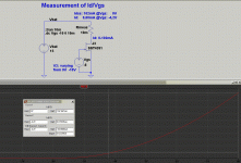
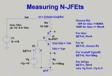
Attached is a easy schem how You can determine the critical values Yourself.
V1 may be a constant voltage power supply or a battery.
Rd is s measuring resistor to determine the drain current.
Choose V1 and Rd so that V(a) is similar to the idle working point of the later application.
A value around 9V suits best.
Vg is a variable negative voltage source. If You only have a constant negative supply at hand You may connect a 1Meg Poti from Vneg to gnd , the wiper going to the Gate.
Rs may be made from fixed resistors or a 1Meg Poti connected as variable resistor.
Following the instructions You can evaluate Idss, Vgs(off) and the Id versus Vgs behaviour.
As the manufacturing process of JFETs includes rather high tolerances the Values of Idss and Vgs(off) vary over a large range.
Manufacturers apply preselection into 2-or 3 Idss classes.
This preselection may already be good enough, as the value of Vgs of the cascoding JFET plays only a minor role for the output offset of the circuit.
Values of Vgs +-0.5V are still fine.
But if You want to achieve lower Vgs tolerances this easy screening method will suffice.
jau
Calvin
the graph in #352 is characteristic for all JFETs.
To evaluate if Your candidate is suitable for the cascoding task have a look in the datasheets and the graphs.
If the DS contains only specs but no graphs, then you can estimate the Vgs at a certain Id in a first aproximation by drawing a straight line in a Id over Vgs graph instead of the real bowed curve.
The end points of the line beeing the Idss value at Vgs=0 and the Id value at Vgs(off).
If the result at a Id of ~8mA is less than -3V Vgs then the JFET should be fine for the task.
Attached is a easy schem how You can determine the critical values Yourself.
V1 may be a constant voltage power supply or a battery.
Rd is s measuring resistor to determine the drain current.
Choose V1 and Rd so that V(a) is similar to the idle working point of the later application.
A value around 9V suits best.
Vg is a variable negative voltage source. If You only have a constant negative supply at hand You may connect a 1Meg Poti from Vneg to gnd , the wiper going to the Gate.
Rs may be made from fixed resistors or a 1Meg Poti connected as variable resistor.
Following the instructions You can evaluate Idss, Vgs(off) and the Id versus Vgs behaviour.
As the manufacturing process of JFETs includes rather high tolerances the Values of Idss and Vgs(off) vary over a large range.
Manufacturers apply preselection into 2-or 3 Idss classes.
This preselection may already be good enough, as the value of Vgs of the cascoding JFET plays only a minor role for the output offset of the circuit.
Values of Vgs +-0.5V are still fine.
But if You want to achieve lower Vgs tolerances this easy screening method will suffice.
jau
Calvin
Attachments
Borbely gave us the general rule for jFET operation:
The Vds applied to the device should be at least 2times the Vp.
A 8mA 2sk170 will have a Vp around the 0.6V to 0.8V
This the 8mA 2sk170 needs > 1.5Vds to operate well. When this minimum voltage is applied you will find that Id ~ 3/4 of Idss.
The cascoding device also has to comply with the same rule.
If a 20mA bf244c has a Vp around 3V to 4V, then it needs > ~7Vds to operate well.
Then use the jig shown by Calvin.
What Vgs does the 20mA cascode device have when passing ~ 3/4 of 8mA?
That Vgs ends up as the Vds being applied to the inner device.
So I have selected at random a 8mA high gm device as the inner and a 20mA low gm device as the outer for the cascoded pair. Check the Vp of both devices (again Borbely shows you how).
When assembled you should check the Vds and Vgs of each device to ensure each receives adequate DS voltage and that the Id is as expected.
Last edited:
Thanks Calvin. I measured Idss of several J109BL-V grades and measures aprox. 70-75mA Idss.
Super explanation Andrew, super thanks. So I have to match for 20mA ?
Super explanation Andrew, super thanks. So I have to match for 20mA ?
Last edited:
... I measured Idss of several J109BL-V grades and measures aprox. 70-75mA Idss.
…
There may be something wrong in your measurement, since 2JS109 V have maximum Idss of 20mA.
Perhaps if more current is required a JFET 'white cathode follower' should be used? It should also improve linearity, saving power is a noble thing too 🙂...
- Home
- Source & Line
- Analog Line Level
- Preamp-Buffers - simple idea