Calvin, I will try and sketch the components that my PRE is consisting of.
First (Image 1): the PSU - section.
230VAC mains enters the case through a SCHAFFNER-filter.
The PE-connector of the filter's output is connected to the metal bottom plate of the case (chassis PE-earth).
I have also connected the R-Core's screen wire to the chassis.
These are the only wires / signals that I have connected to the chassis!
The Schaffner-filter is followed by a DC-hum filter.
(I have already bypassed the hum-filter, but this did not change anything.)
The used R-Core provides 2 x 9VAC @ 350mA each and 2 x 18VAC @ 650mA each.
The R-Core connects to the PSU shown in image 2.
The PSU consists of 3 sections: a +5VDC / +8VDC on the left side for the passive PRE, a +5VDC for the DAC and a +/-18VDC for your buffer on the right side.
The "Buffer-PSU" is using a traditional LM3x7 ddesign (see image 3).
The 3 sections of the PSU work "independently" from one another.
The GNDs of the 3 sections are not connected to each other.
The source signals pass through a selection relay (see image 4), the LDR-attenuation and the mute relay.
The source's return-wire is not connected to GND on the passive PRE-PCB.
I have placed a 3-pole connector (Out-Left, Out-Right, Signal Return) on the output of the mute-relay.
When I run some wires from this connector to the RCA connector in the back-plane and connect an amplifier to it, everything works fine.
When I connect the output of the mute-relay to the buffer (see pink arrow on image 5), I have a persistent awful hum.
The funny thing is:
- I am able to perfectly adjust your buffer
- Looking at the buffer's output with my oscilloscope, I see very well shaped sine and square waves.
What could be the reason for this strange behaviour?
Best regards - Rudi
P.S.: The buffer-PCB is shown in post #617.
Your schematic is wrong.Joshua: the hum is present, even if no input (CDP, ...) is connected to the PRE (I need to verify this once more and ask my DIY-friend Hans).
I have placed 2 x 100µF capacitors on the buffer PCB near the PSU-connector (have a look at the image in post #617 please).
Best regards - Rudi
It shows the two terminals at the extreme left connected to the OUTPUT at the extreme right.
The transformer CT MUST be connected to the INPUT of the smoothing capacitors bank. i.e. connect SV4 -2 and SV4 -3 direct to the junction between C1 and C8. BUT also twist the AC wires together from transformer to rectifier and twist the DC wires together from rectifier to smoothing capacitors. The CT wire must be included inside that twisted group.
The 3pin regulators are also wired wrongly.
The adjustable VR must connect to the output node, as must it's capacitor.
The +ve regulator MEASURES the output voltage using TWO connections, one on the +ve side of the output and one on the Zero Volts side of the output.
If one of these wires reads the wrong voltage, then the regulator will give the wrong output.
DO NOT let the regulator read the ripple on a shared Zero Volts line.
Last edited:
It's part of the Thiele Network that virtually all amplifiers use to help with maintaining stability.
However, using an inductor alone to drive a reactive load will result in ringing and that ringing frequency will depend on the L & C values.
To suppress the ringing you add resistance to damp out the resonance.
For typical speaker loads of 4ohms to 8ohms we generally use 0.5uH to 6uH with a parallel damping resistor from 1r0 to 10r0.
I think the top end values of both these two ranges are far too high for normal speakers. I suggest 0.5uH to 1uH parallel with 1r0 to 5r0 as a reasonable range for normal speakers.
Most of the above is relevant to power amps.
Here we are dealing with a buffer, which is the active part of a preamp, not connected to speakers or any other reactive load.
…
The transformer CT MUST be connected to the INPUT of the smoothing capacitors bank. i.e. connect SV4 -2 and SV4 -3 direct to the junction between C1 and C8. BUT also twist the AC wires together from transformer to rectifier and twist the DC wires together from rectifier to smoothing capacitors. The CT wire must be included inside that twisted group.
Those are good points, however from the schematic posted it's impossible to know how the physical wiring is done.
The 3pin regulators are also wired wrongly.
The adjustable VR must connect to the output node, as must it's capacitor.
The +ve regulator MEASURES the output voltage using TWO connections, one on the +ve side of the output and one on the Zero Volts side of the output.
Look again at the posted schematic, it's done this way. The adjustable VR is connected to the output node via 2 series resistors, it cannot be connected directly to the output.
...
DO NOT let the regulator read the ripple on a shared Zero Volts line.
What do you mean by it?
That is why when the question about 10uH came up I thought 10uH sounded about right for a Buffer that is driving a much higher impedance than a typical 4 to 8ohms speaker.Most of the above is relevant to power amps.
Here we are dealing with a buffer, which is the active part of a preamp, not connected to speakers or any other reactive load.
I don't agree that <1uH is correct.
The Buffer IS connected to a reactive load.
Any parasitic reactances, or deliberately added reactances, are a LOAD on the Buffer.
The Buffer is designed to cope with those inadvertent and deliberate reactances.
Last edited:
The sch shows the GND symbol attached to SV4 -2 and to SV4 -3Those are good points, however from the schematic posted it's impossible to know how the physical wiring is done.
The sch also shows the OUTPUT of the regulator attached to GND.
The sch tells you where to make the connections. Rudi said
This points to a wiring error.Originally Posted by Rudi_Ratlos
Joshua: the hum is present, even if no input
This is yet another example where using the same term for all "grounds" leads to ERRORS. Make the diagrams unambiguous by showing the correct unambiguous terms for each different terminal.
The adjustable VR is connected to the "ground" line (or Zero Volts line) between C2 and C11.Look again at the posted schematic, it's done this way. The adjustable VR is connected to the output node via 2 series resistors, it cannot be connected directly to the output.
This point is at a different voltage from the INPUT to the regulator and at a different voltage at the OUTPUT from the regulator.
If you need the regulator to READ the OUTPUT voltage, then the VR must be connected to the NODE that is at the SAME voltage as the output. i.e connect VR and it's capacitor to the output node.
the long wire from the CT to the OUTPUT carries variable current.What do you mean by it?
That variable current passing through impedances generates variable voltages.
The voltages at the beginning and in the middle and at the end are NOT the same.
Stop calling everything "ground".
Give every different Return wire it's own unique label.
BTW there is a paper liked in this Forum from a decade or more ago describing precisely this 3pin regulator problem and describes exactly how to avoid 3pin regulator wiring errors.
As usual it's a lack of research on the part of our Members that leads to many of the errors we see being repeated time after time.
I have written about this problem before and I have mentioned that old paper before.
Last edited:
…
I don't agree that <1uH is correct.
…
Whether you agree or disagree, it works very well in actual buffers, connected to actual sound setups.
The sch shows the GND symbol attached to SV4 -2 and to SV4 -3
The sch also shows the OUTPUT of the regulator attached to GND.
The sch tells you where to make the connections. Rudi said This points to a wiring error.
…
Your quibbling is irrelevant to the actual PSU. Rudi wrote me in a PM that the PSU is actually wired as you wrote it should be, not as you read the schematic.
At times schematics refer only to the electric connections, not to the actual, physical wiring. This is one of those cases.
Anyhow, the very same PSU works very well on one setup, while there is a hum on another setup.
If you insist on quibbling, good luck and fare well.
@Stormsonic:
The different GNDs of DAC, PRE and Buffer PSU are not connected to one another.
AUDIO GND (Signal Return) is not connected to either DAC or PRE GND.
It connects of course on the entry to the buffer PCB with the buffer - PSU - GND (have a look at image 4).
Best regards - Rudi
P.S. Joshua: I have sent you a PM.
Rudi
In one box, you can't have different GND's, i.o.w, all your GND's must be on the same electrical potential. If they are not, current will flow as soon as they are connected together.
Draw connection diagram (not schematic!) of your present situation on paper, then trace current flow (paths) with pencil.
Last edited:
Getting back to my question, will these inductors work in parallel with the 27 ohm resistors?
RLB1314-100KL Bourns | Mouser
Thanks...
RLB1314-100KL Bourns | Mouser
Thanks...
Getting back to my question, will these inductors work in parallel with the 27 ohm resistors?
RLB1314-100KL Bourns | Mouser
Thanks...
It looks like this one 78F1R0K-RC J.W. Miller | Mouser is better suited.
It looks like this one 78F1R0K-RC J.W. Miller | Mouser is better suited.
Thank you, Joshua.
Those are even less expensive than the 10uH I linked to.🙂
#628 #630 !!
And your point is...??? That a 1uH fixed inductor will not work?
And your point is...??? That a 1uH fixed inductor will not work?
Just the other way around; the suggested inductor is about 1uH. This is what Calvin said in the posts he referred to.
Thanks to the assistance of HESENER the problem that I have reported about my PRE / CalvinBuffer - build in post #632 has finally been resolved.
I have been using 470µF - 47Ohm - 1000µF CRC-filters in the buffer's +/-18VDC PSUs.
When I calculated the filters' resistor's value (47Ohm), I have anticipated a too small value of current flowing through the power rails.
The actual voltage drop across the filter's resistors has then been so large that the minimum input LM3x7 voltages have not been matched resp. have been "on the edge".
So the LM3x7 had a "tendency to oscillate".
I myself have not been aware of this problem, when I built the prototype.
Maybe the JFETs that I have used have a very low IDSS or the primary voltage in Hamburg is rated at 235VAC whereas in Stuttgart ..
Anyway: substituting the filters' resistors by a 4R7 value remedied all of my problems.
Thank you once more, Alfred.
Best regards - Rudi_Ratlos
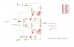
Calvin, it looks like your buffer cannot be as easily used as a "general buffer" as I thought (not being used in your Paradise phono stage board) - as I have told in my post above.
Being connected between a LDR - attenuation and a SYMASYM (which has an input impedance of about 20K), it shows a tendency to oscillate on its output.
Can this oscillation be remedied by increasing the value of the compensation capacitors (indicated by the red circle)?
And another question: as +/-18VDC PSU for your buffer I am using a LM3x7 "Tracking Pre-Regulator" PSU.
There is - I admit - a ripple of about / lower 1mV on the voltage rails.
Is my PSU "good enough" for your buffer or does it need a "more accurate / more ripple-free PSU"?
I am looking forward to your answer - best regards - Rudi
Attachments
Last edited:
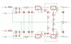
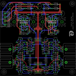
Calvin,
this is how your buffer will eventually look like - as least in my eyes / ears!
TPR-PSU and your buffer on a single 100x100mm PCB!
Best regards - Rudi
P.S.: Well: and I am quite sure that no other buffer that I have listened to so far (Diamond-Buffer, JLH-Buffer, Pass-Buffer, ...) can compete to it.
Attachments
Last edited:
Rudi,
Just small comment, I am not sure if this can be of any help but I would suggest to review value of the R6 and R11 in your PSU. The purpose of this C4/R6 and C6/R11 circuit is to dump any eventual tendency to oscillation in PSU. As per information I found for 1uF capacitor there should be a few ohms value (3R3?) instead of 3k3.
Thanks for your PCB design!
rgds
-jacek
- Home
- Source & Line
- Analog Line Level
- Preamp-Buffers - simple idea