I completely agree that the performance of both, Calvin and CFP2 is really very good!
I am just trying to understand the differences between the Calvin buffer ("real live" performance close to simulation) and the CFP2 (which simulates even better but "real live" is a little bit inferior): is this an effect of board design, parts variation,...?
Anyway I will now build two boards of both and do some listening (thats what counts in the end, isn't it ?) probably at the Frickelfest light 2014 together with e.g. Joachim and maybe Frans (?) 😀
Regards, Daniel
PS: just a side note: the THD I measure with my soundcard with the calvin buffer is better than loop through 😀
Hi,
the simu Models of the BC8xx seem to sim better than in real ;-).
Btw. if load impedance is >>1k the simpler Hybrid CFP (1x NJfET, 1x PNP) sims equally well.
jauu
Calvin
ps
the simu Models of the BC8xx seem to sim better than in real ;-).
Btw. if load impedance is >>1k the simpler Hybrid CFP (1x NJfET, 1x PNP) sims equally well.
jauu
Calvin
ps
Ya know that CFP stands for Calvin-for-President eyyhh? 😀😀better than loop through 😀
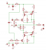
What is going on with my layout ...
Gentlemen, since I have been in need of a buffer for my VCPre-preamplifier (just to drive a 1m long RCA-cable and to be able to connect to any low-impedance amplifier), I did a layout of my own
of the CALVIN's buffers (I will never connect it to a Phono-Pre - since I do not have) and powered it from a "DIY PSU" (LM7818/LM7918) of my own.
I have shortened the input and adjusted the output to be able to show less than 1mV - DC on it.
I cannot believe!
What am I doing wrong?
Best regards - Rudi_Ratlos
Attachments

Last edited:
Rudi,
Upper side of R5 should be connected to Vdd, not at the midpoint of R1/R2.
DC balance can't be reached correctly the way you draw it.
Upper side of R5 should be connected to Vdd, not at the midpoint of R1/R2.
DC balance can't be reached correctly the way you draw it.
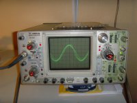
Rellum, even after correcting the R15 connection, my problem persists.
I feed the input of my pre-amp with a 1 KHz stable sine wave, but the output of the buffer is showing an instable, dithering sine wave.
When I stop the input, a saw-tooth wave is still present.
Best regards - Rudi_Ratlos
I feed the input of my pre-amp with a 1 KHz stable sine wave, but the output of the buffer is showing an instable, dithering sine wave.
When I stop the input, a saw-tooth wave is still present.
Best regards - Rudi_Ratlos
Attachments
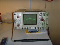
Problem solved!
Andrew: I do not need a new DMM. I need a pair of new eyes. My ones are growing old. Do you have a spare pair for me?
Best regards - Rudi
Andrew: I do not need a new DMM. I need a pair of new eyes. My ones are growing old. Do you have a spare pair for me?
Best regards - Rudi
Hi,
well the shown schematic was wrong, as rellum already remarked.
Compare to #87.
After the wrong schem only the 75R remain effective as Vbe-generating Drain-load of the JFETs. As the JFETs will run a bit hotter than intended, but still only on a few mAs the voltage drop over the 75R will be less than the required ~600-700mV to open up the bipolar transistor.
It will be cut off.
As such the positive branch will contribute only the JFET´s current, while the lower branch works as intended at its idle current.
Hence there will be a lot of current through the connected load --> high Offset voltage.
@Rudi.
With the fixed set of 105/75Ohms the degree of modulation of the negative branch is fixed.
You can make it trimmable with an arrangement as in #190.
Replace R1,R2 by a parallel of fixed R and a Pot.
Choose the fixed resistor the same as in the negative branch (220R) and the Pot half the value of the negative branch (1k)
Connect the lowest load impedance You want to drive and adjust the pot for same, symmetrical current amplitudes into the load (measure voltage swing over R6 and R11).
jauu
Calvin
Last edited:
BTW, I also had oscillations when using LSK389C. With BF862 it is running stable.
regards, Daniel
regards, Daniel
Hi,
interesting to know.
The LSK389C certainly has higher capacitance.
The compensation caps would need to be a bit higher in value to tame the oscillations.
Was the input bandwidth limiting filter as suggested and the output inductor installed?
A lower bandwidth limit and/or a higher inductor value could also help.
jauu
Calvin
Yes, input Filter was 270R + 470p as suggested, output Zobel 27R + 1µH, compensation cap 150p.
regards, Daniel
regards, Daniel
I used lsk170 and j111 and had no oscillations.
But, as reported earlier, I did have to modify many resistor values to get the currents about right.
I used 10uH as in a BoM.
And added a 100k load resistor just in case the output was disconnected.
But, as reported earlier, I did have to modify many resistor values to get the currents about right.
I used 10uH as in a BoM.
And added a 100k load resistor just in case the output was disconnected.
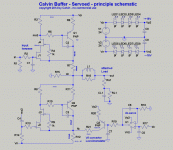
Hi,
due to a recent request I thought about a new variation to the Calvin-Buffer. 😉
It was asked for higher supply lines and a dc-servo.
Somehow it didn´t occur to me that someone would want to have a DC-Servo with the Buffer, as any (static) Output Offset could be trimmed away so simply with the Poti.
As part of a circuit like the Paradise there was also no need for a servo dedicated to the Buffer itself.
Also higher supply lines -while indeed increasing output voltage headroom (for what purpose?)- are rather increasing heat power losses to the edge or above the SOA of the cacoding JFETs and bipolars, especially with the SMD devices I prefer.
Anyway here´s what came up with.
One can easily see the known topology of the Calvin Buffer.
What differs is, that there´s no poti in parallel to R8 anymore, that had been used to trim the output offset to 0V.
Instead one OPAmp, one Transistor and a few associated parts have been added.
The OPAmp senses any offset voltage at point dc.
Now when having a corrective voltage at the output of the OPAmp, the Q remained where to feed it into?
If there were a series ac-coupling capacitor at the Input, one could feed the corrective voltage right behind the cap into the input -using a inverting servo stage.
If not and one wishes to dc-couple the whole Buffer, feeding the corrective signal directly into the Input could interfere with a DC-Servo of a preceeding stage/device.
Besides I´m not a friend of feeding a corrective signal directly into a sensitive signal point.
What the Poti in parallel to R8 did, was to change the overall Bias current flowing through R12.
The voltage drop over R12 is at the same the Gate-Source voltage of J2 and as such defines the current through J2/J3 and Q2.
That brought me to the idea that one just needs to modify the idle voltage drop over R12.
This can be achieved by making R12 a bit smaller in value than R7, the resistor with the same function in the upper half of the circuit.
Beeing smaller in value the current through R12 is higher and so is the current in the trace from point dc to node R8/R11
If the currents through R7 and that trace were equal the output Offset would be 0V.
To get these both currents equal one needs to give the ´excess current´ through R7 a own dedicated path to a more positive potential than at point fb.
This path is formed by R21-Q3-R20 towards the positive OPAmp supply.
Q3 converts the OPAmps corrective output voltage into the required current.
I chose parts values so that Q3 takes over 0-10mA with a idle value of ~5mA (~1/10 of the overall Bias current).
R19/C7 form a post-filter for the servo, reducing artefacts from out of the servo.
The supply voltages for the OPAmp and Q3 are generated by LED-strings and Caps, reducing the +-24V supplies to ~+-16V.
If parts are matched well, the servo may filter out input offset voltages of up to +-15mV.
In praxs the range will be lower, but then should no dc feed into a amp input anyway.
So far the circuit is just Sims, but You may dare and give it a try 😉
jauu
Calvin
Attachments
Calvin,
Do you think your buffer can drive 100 ohms load well?
I have 25 feet (about 8 meters) between my preamplifier and power amp. I'm thinking of using 50ohms RF coax cable and have it terminated with 50 ohms at the power amp end. Preamp/buffer will have 50 ohms series output resistor. This will be total of 100 ohms load for preamp/buffer.
Thanks,
gurevise
Hi,
in principle, yes 😉
It depends on the required maximum output voltage level and the idle current of the Buffer.
Joachim Gerhard has checked that quite early in this thread.
IIrc the idle current was somewhere between 50 and 70mA and various load impedances were tested down to 15R.
But let´s do some quick evaluation:
Taking 1Vrms as typically sufficient output voltage this equals +-14mA of load current.
As rule of thumb the THD in SE circuits like this buffer remains low if the bias is approximately five times or more the load current.
14mA x 5 = 70mA.
4Vrms (= +12dB) into 100R equals +-57mA peak signal current.
So, 70mA idle current should suffice to drive a 50R transmission line system with the negligable THD the Buffer is known for and offering at least +12dBV of headroom with increasing THD.
jauu
Calvin
Last edited:
- Home
- Source & Line
- Analog Line Level
- Preamp-Buffers - simple idea