The way I do my pcb is that even if I had a pdf/jpg/gif file of the tracks, I who draw my own board with my pcb software which can generate gerber files for the different layers. I guess that the 'outline milling profile' cannot be generated automatically from a gerber files of the tracks by your software, can they? If that is the case, that would mean redundant work (if you may say that).
I can understand that the milling process is just to isolate the tracks but won't go as far as milling all the unwanted area away as in etching. That would mean giving too much work to the router.
I can understand that the milling process is just to isolate the tracks but won't go as far as milling all the unwanted area away as in etching. That would mean giving too much work to the router.
well after lots of different tests, I've come to the conclusion that Q's layout can not be routed!
Some of the tracks are just to small.
I suppose its time to drag the light box out!
Some of the tracks are just to small.
I suppose its time to drag the light box out!
Quasi, Is there any chance you could send me the original artwork of the 10 fet board (before converting it to a pdf)?
I was hoping to have something which I can modify to increase the track width.
I was hoping to have something which I can modify to increase the track width.
Hi matth,
That's exactly what I am talking about. No matter how nice or well the original design is, there is always some ways that it can get outside of your own coverage. I just try to get more controll of the stuff by laying the pcb of my own. There is also 1 terrible thing about this : I am always changing me layout, trying to improve somehow.
That's exactly what I am talking about. No matter how nice or well the original design is, there is always some ways that it can get outside of your own coverage. I just try to get more controll of the stuff by laying the pcb of my own. There is also 1 terrible thing about this : I am always changing me layout, trying to improve somehow.
Re: !!! 1000 POST FOR QUASI !!!
Here is the original artwork, but you will need Sprint Layout to modify it. http://www.diyaudio.com/forums/showthread.php?postid=978310#post978310
Yeah 1000 posts indeed. Bugga though that I wasn't the one to post #1000. Oh well maybe I'll get to do #10,000.
There are obviuosly unlimited layouts that can be done for this schematic. My thoughts for anyone doing there own are mainly these;
Keep the output well away from the input.
Apply star earthing as much as possible. In my layout you'll see two obvious "star earths".
Power supply capacitor tracks should always run away from the voltage source and never between the voltage source and the powered section. E.g; the positive track from the fuse to the capacitor runs in the opposite electrical direction to the track that feeds the FETs.
Keep tracks short and avoid parallel paths (esp. between high current and low current paths).
And it should look nice.
Finally the performance of this amp has quite a lot to do with the actual layout I have used.
There are probably others, but I just got off a plane....and I'm beat.
Cheers
Q
matth said:Quasi, Is there any chance you could send me the original artwork of the 10 fet board (before converting it to a pdf)?
I was hoping to have something which I can modify to increase the track width.
Here is the original artwork, but you will need Sprint Layout to modify it. http://www.diyaudio.com/forums/showthread.php?postid=978310#post978310
TomWaits said:Goodtimes!
Yeah 1000 posts indeed. Bugga though that I wasn't the one to post #1000. Oh well maybe I'll get to do #10,000.
bigpanda said:Hi matth,
That's exactly what I am talking about. No matter how nice or well the original design is, there is always some ways that it can get outside of your own coverage. I just try to get more controll of the stuff by laying the pcb of my own. There is also 1 terrible thing about this : I am always changing me layout, trying to improve somehow.
There are obviuosly unlimited layouts that can be done for this schematic. My thoughts for anyone doing there own are mainly these;
Keep the output well away from the input.
Apply star earthing as much as possible. In my layout you'll see two obvious "star earths".
Power supply capacitor tracks should always run away from the voltage source and never between the voltage source and the powered section. E.g; the positive track from the fuse to the capacitor runs in the opposite electrical direction to the track that feeds the FETs.
Keep tracks short and avoid parallel paths (esp. between high current and low current paths).
And it should look nice.
Finally the performance of this amp has quite a lot to do with the actual layout I have used.
There are probably others, but I just got off a plane....and I'm beat.
Cheers
Q
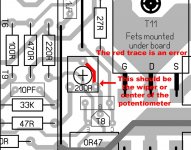
Sorry Q, I don't mean there is something wrong with your board layout. All I am saying is that if I am to make a pcb (which is what I am starting to do now), I won't just take your pdf file and try to make a film or whatever I need to proceed making the pcb. First I will lay the pcb with my own pcb software /w your original as the blueprint, then looking for places that I may have modification to suite my own need. There is always space for improvement to fit your taste. Hope I did not offend anyone.
Not offended at all, indeed I am interested to see modified boards that suit different needs, I.e, cases, power needs, available components (TO3, TO220) etc.
I just wanted to contribute that some design rules are important to ensure a good result.
I just wanted to contribute that some design rules are important to ensure a good result.
Sprint
Q, did you ever post the Sprint schematic layout, can you post it?
That software plays elevator music when you install it 😀
Shawn.
Q, did you ever post the Sprint schematic layout, can you post it?
That software plays elevator music when you install it 😀
Shawn.
schematics
Hi Quasi
Can you send me all about the latest version of your project ?
My e-mail is sonsom@rediffmail.com. I am a new member.
Thanks and Regards
Sony Soman
Hi Quasi
Can you send me all about the latest version of your project ?
My e-mail is sonsom@rediffmail.com. I am a new member.
Thanks and Regards
Sony Soman
Re: Sprint
For Splan users.....here is the schematic.
Cheers
Q
TomWaits said:Q, did you ever post the Sprint schematic layout, can you post it?
That software plays elevator music when you install it 😀
Shawn.
For Splan users.....here is the schematic.
Cheers
Q
Attachments
Re: schematics
Hi Sonsom, You have mail.
Cheers
Q
sonsom said:Hi Quasi
Can you send me all about the latest version of your project ?
My e-mail is sonsom@rediffmail.com. I am a new member.
Thanks and Regards
Sony Soman
Hi Sonsom, You have mail.
Cheers
Q
Hi Quasi
Can you send me the latest version of pdf file of your project ?
My e-mail is tsamuel0573@yahoo.com.hk.
Thanks and Regards
Samuel
Can you send me the latest version of pdf file of your project ?
My e-mail is tsamuel0573@yahoo.com.hk.
Thanks and Regards
Samuel
Low Voltage Quasi
If I built some smaller Quasi's running at -/+ 22VDC Rails will the existing pre and drive circuitry work well. Or do I need to change some resistor values and use some different transistors?
Jah.
Shawn.
If I built some smaller Quasi's running at -/+ 22VDC Rails will the existing pre and drive circuitry work well. Or do I need to change some resistor values and use some different transistors?
Jah.
Shawn.
Re: What is a Sprint schematic layout
sPlan is a schematic program
Sprint Layout is a printed circuit board layout program
Both are by ABACOM
I liked Q's boards so I ordered these programs because it is what he used to make his quasi PCBs.
Cheers,
Shawn.
ppcblaster said:What program uses it? Thanks
sPlan is a schematic program
Sprint Layout is a printed circuit board layout program
Both are by ABACOM
I liked Q's boards so I ordered these programs because it is what he used to make his quasi PCBs.
Cheers,
Shawn.
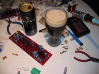
Beers & Boards go so well together...
Another round of PCBs coming together. 🙂 Toshiba 2SK1530 samples were shipped bulk by BOAT across the Ocean and I will not see them for some time! 🙁 I looked at some offshore knock-offs today and they were obviously poor quality...I will wait and finish the case(s). The knock-offs were like $4 each, much lower than the 1's and 2's price of the real device which varies from $10~$15 US or CAN funds each.
Shawn.
Attachments
- Home
- Amplifiers
- Solid State
- Power amp under development