Hi qsa,
Thankyou replaying. Here still i use transformer due to non availability of SMPS or huge cost for shipping to india.
vijay
Thankyou replaying. Here still i use transformer due to non availability of SMPS or huge cost for shipping to india.
vijay
Hi qsa I like this circuit 🙂 also please send me copy off pcb drawing, schematic and part list thanks .juancacerce@hotmail.com
pcb
hi qsa please send me the latest nmos pcb desin ,control board and smps khalsaaudiocenter@yahoo.com thanks
hi qsa please send me the latest nmos pcb desin ,control board and smps khalsaaudiocenter@yahoo.com thanks
Hi QSA,
Can I have a pdf copy of your board I plan to build for my personal use. I already sent you an email. My email - presbel1950@hotmail.com.
Thanks.
Rey
Can I have a pdf copy of your board I plan to build for my personal use. I already sent you an email. My email - presbel1950@hotmail.com.
Thanks.
Rey
Hi guys
have a question,.. who did build NMOS since today too and had similar experience...
Input differential Transistor T1 T5 (2SC2240 or 2SC1845) are hot
after changed R5 18K from quais schematic to 40 K temperature from T1 and T5 (2SC2240 or 2SC1845) is low
I think 18K in original design is to low
willl send latest schematic and PCB LAYOUT at weekend
attachment latest NMOS design
changes are R6 from 18 to 40K reduces power dissipation in differential input stage
Industrial DIY PCB are available
changes are R6 from 18 to 40K reduces power dissipation in differential input stage
Industrial DIY PCB are available
Attachments
R6 controls the dissipation in T3.
R7 controls the dissipation and the gain of T1 & T5.
Check the voltage across R7 and check it's value.
R7 controls the dissipation and the gain of T1 & T5.
Check the voltage across R7 and check it's value.
attachment latest NMOS design
changes are R6 from 18 to 40K reduces power dissipation in differential input stage
Industrial DIY PCB are available
Hi Qsa,
Sorry but I disagree with your first stage configuration. Using a LED as the reference for T3 means that about 5.5mA will flow through R7 and R6. The voltage across R6 if it is 40k will be 220v (or at least try to be). This is more than the rail voltage meaning there is no voltage left for T3. So we do not have a proper constant current source (CCS). Even 18k is too high for 5.5mA as this will try to have 99 volts across it.
If I were you I would reduce the CCS current to 3mA by replacing R7 with a 390 ohm resistor. Then replace R6 with an 18K resistor. I would also replace R4 and R12 with 390 ohm resistors and drop the voltage across these to 0.6 volts (you currently have 1.3 volts here).
In the second stage CCS your choice of 47 ohms as R19 means that 25mA will flow through T7 and T8. This amouns to a dissipation of 4 watts and is completely unnecessary. I would change R19 and R15 to 100ohms and reduce the current through this stage to 12mA.
Cheers
Q
Last edited:
Hi Quasi
Thank you for assistance, will change it and test
actually there is a new posting
http://www.diyaudio.com/forums/solid-state/162408-900w-h-class-pa-amp-limiter-5.html#post2112754
Im very interested to add Class H for NMOS
Thank you for assistance, will change it and test
actually there is a new posting
http://www.diyaudio.com/forums/solid-state/162408-900w-h-class-pa-amp-limiter-5.html#post2112754
Im very interested to add Class H for NMOS
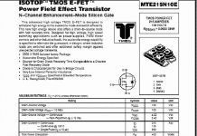
Hi
I have some MTE215N10E
Can I use them for the Quasi Nmos 200 ?
Thanx
Paul
Note that they are only 100V devices, so you have to keep your supply to +/-50V maximum. Also, given their high current nature and low rdson, I would expect them to have very large capacitance, so you could have problems at high audio frequencies. No harm in trying them though!
Hi quasi,
Is it possible to post the pcb layout for the PSU you made for this amplifier
http://www.diyaudio.com/forums/solid-state/43331-power-amp-under-development-15.html
I need something to print on laser printer.
Thank you!!
Is it possible to post the pcb layout for the PSU you made for this amplifier
http://www.diyaudio.com/forums/solid-state/43331-power-amp-under-development-15.html
I need something to print on laser printer.
Thank you!!
Hi qsa please send me the latest nmos pcb desin ,control board and smps malbasicradan@gmail.com thanks
Hi quasi,
Is it possible to post the pcb layout for the PSU you made for this amplifier
http://www.diyaudio.com/forums/solid-state/43331-power-amp-under-development-15.html
I need something to print on laser printer.
Thank you!!
Sorry about the delay. You can find a layout here.
Nmos & Nbip series (Quasi's DIY Audio Site)
Cheers
Quasi
Thanks Andrew, it's pretty easy with the software I use. Anyway I wish I had more time to do more...oh well.
Cheers
Cheers
350 mk2
how about replacing the 5.1v Zener with a pair (or 3) of ~1.9V LEDs?
Maybe combine R11 & R12 and use a 36K with no connection to ground.
What is the design current through R11 & R12?
What about hFE recommendations for T1, T4 & T6?
1.8/hFE T1 + 1.8/hFE T4 = 10/hFE T6.
But this requires a very high gain T6. Instead add a resistor from +ve supply rail to junction of T1+T4 bases. This makes a better job of balancing the currents coming out of the mirror.
Last edited:
- Home
- Amplifiers
- Solid State
- Power amp under development