just to inform you guys that i already made the nmos500. all parts, pcb are based on quasi's published version (http://www.adam.com.au/cgpap/QuasiWeb/) except the irfp450s, instead i used the 460s. i don't have the right measuring tools but the audio output is great, so far. i am using a 45-0-45 VAC power transformer.
Nmos350 Mk II
.
Greetings,
Attached is the schematic for the Nmos 350Mk II.
In this schematic some contributors will recognise their own suggestons for improvements. To you I say a big thank you.
Comments and suggestions for further improvement are of course welcome.
Major changes to date include;
- Cascode second stage to improve the linearity and speed of this stage.
- replacement of the 100 ohm resistor in the driver stage with 4 diodes.
- LED based constant current source with enhanced filtering.
- fuses shifted outside of the output driver gate loop.
Cheers
Quasi
Attachments
does C5 connect to negative rail or to ground?
R7 is too large.
18k and 4mA drops 72V. I suggest 8k2 or 9k1
Output FET base resistors?
Is C9 upside down?
R7 is too large.
18k and 4mA drops 72V. I suggest 8k2 or 9k1
Output FET base resistors?
Is C9 upside down?
does C5 connect to negative rail or to ground?
Wow ,can't believe I missed that one..horrible PSRR..
Other changes/improvements R11/12 6K8 for 5 ma to
RED led, Eliminate R7 entirely,change R8 to 330R for 4mA CCS.
(have 4 of these working at home at the moment.)
Also, use nonpolar EL for C9 (still small, bye bye D2/3)
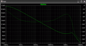
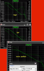
and I always wondered about C11 ,at 10p , way over-
compensated ,2 pf works the best.
At 10 p , huge "bump" at 1MHZ (phase margin and OLG)
almost a 2 pole response.
(see below)
OS
Attachments
R7 may have to go to 240r or even 220r to get 4mA of tail current. My red LEDs and BC5xx leave ~900mV across the current setting resistor.
How do you check balance in the LTP when that VR1 is in there?
Os,
please post comparative graphs for 0pF, 2pF and 10pF, so that we can recognise what happens here.
How do you check balance in the LTP when that VR1 is in there?
Os,
please post comparative graphs for 0pF, 2pF and 10pF, so that we can recognise what happens here.
Im missing Gate resistors for the mosfets ? normally paralleling mosfets oscillating, im wondered working stable
Thanks AndrewT
I'm glad someone's awake......
Corrections made. I'll play with the LED forward voltage and subsequent constant current in the prototype.
Cheers
Q
I'm glad someone's awake......
Corrections made. I'll play with the LED forward voltage and subsequent constant current in the prototype.
Cheers
Q
C5 still goes to ground.. full negative rail ripple across led.🙁
BTW , I must thank you, quasi , for my start at DIY amps...
brother of quasi still lives (with better CCS)
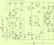
Soon I wil replace with the "beast" .. if you can use any ideas
from it (see below) I owe it to you. It runs in the real world with
BJT's now ,so It is proven.. I'm on the diamond buffer "kick' now.
so feel free to use it. CFP and balanced operation are its
strengths and I am only going to use it for my 1 sub.
(see attachment)
OS
BTW , I must thank you, quasi , for my start at DIY amps...
brother of quasi still lives (with better CCS)
Soon I wil replace with the "beast" .. if you can use any ideas
from it (see below) I owe it to you. It runs in the real world with
BJT's now ,so It is proven.. I'm on the diamond buffer "kick' now.
so feel free to use it. CFP and balanced operation are its
strengths and I am only going to use it for my 1 sub.
(see attachment)
OS
Attachments
Does R13 need to connect to Ground?
Could a single resistor replace R13 + R11?
What about replacing D1 with three series red LEDs?
C5 is back to front. Zoom in and it becomes visible.
What about adding + symbol beside each electrolytic?
Could a single resistor replace R13 + R11?
What about replacing D1 with three series red LEDs?
C5 is back to front. Zoom in and it becomes visible.
What about adding + symbol beside each electrolytic?
Does R13 need to connect to Ground?
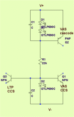
that is a good idea ,andrew. Run both cascode and the 2 CCS's off the same bias string , no ground reference,less parts, better PSRR.
See attachment.
Attachments
Samuel Jayaraj said:Quasi, is VR2 connected the right way?
Ummm....no it's not. Thanks Samuel.
Corrected schematic attached.
Cheers
Q
Attachments
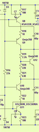
C11 should be between base T5 and the VAS, collector T7 or T9. The purpose is to let the output stage run without feedback at very high frequencies. The value should probably be more 33-100 pF.
peranders said:C11 should be between base T5 and the VAS, collector T7 or T9. The purpose is to let the output stage run without feedback at very high frequencies. The value should probably be more 33-100 pF.
That's another way of doing it.
The capacitor shown gives phase lead and is another (IMO better) way of doing it, at least for an amp relying mostly on miller compensation.
- Home
- Amplifiers
- Solid State
- Power amp under development