What the ,,,,?
I did a search and the ONLY location for the search string is your post.
I guess you never ever mistyped while posting 🙄
AndrewT Who?
See above.
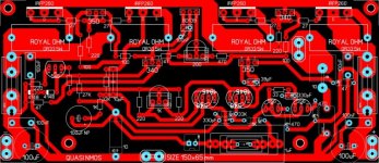
FWIW: http://www.diyaudio.com/forums/atta...lopment-nmos-class-ab-2709201-small-power.pdf
Some help plse
I have build the nmos350 with three pairs IRFP460 on the outputs. I have VGS matched the fets and with the initial setup with 10 ohm resisters in the place of the fuses and bulbtester in circuit I can set the offset to 0V and the bias to 10 mv over the 0.33 source resistors. But the problem arises when I remove the resistors and inline testbulb of 40W. The bias pot is 220 ohm and at its lowest setting I can set the bias to about 50 mv and it must go down to 10 mv. I cannot get it any lower. Can I increase R13 from 470 ohm to 560 Ohm or should I decrease it to say 390 Ohm without it having a detrimental influence on the working.
Help will be appreciated.
The bias current should be measured as a voltage across the 10 ohm resistor which you have placed in place of the fuse (0.3V per FET pair). The voltage should be 0.9V for your setup (three pairs). Adjust this using VR2.
Hari
Hari
jethari, thanks for the reply.
I know how to set that up and I do adjust the module like that but when the 10ohm resister and bulb limiter is removed then it is impossible to get the voltage lower than 50mv over the .33ohm source resistors. My problem is that VR2 does not have enough lower reach which means at it lowest setting the voltdrop over the source resistors is 50mv i.s.o 10mv. That is why I wonder if I increase R13 to 560ohm if I then would be able to adjust VR2 to get the lower bias over the source resistors. Any ideas anybody ?
😕
Vrystaat, I'm not sure if Quasi mentions about measuring voltage across the 0.33 ohm resistors during the initial setup. He only mentions adjusting the bias current using the temp resistor in place of the fuse. In fact, I have made the two pair version of the NMOS and I only did the adjustment using the 10 ohm resistor. Additionally, I also connected an ammeter in place of the fuse and cross checked the bias current. The most important point is to ensure that there is no DC at the output.
Hari
Hari
check the values of R13, R14 and Vr.
470/{200+47} = ~2
The Vbe multiplier minimum voltage will be around 3times 0.65V i.e. ~2V.
Take off 1.2V for the driver Vbe and you have only 0.8V available to turn on the output mosfets.
They will NOT turn on.
Check your resistances.
Check your voltages.
There is an error in the wiring of the Vbe multiplier.
The base of T8 must be wired to the top of R14.
This is to prevent the multiplier blowing up the output stage if the wiper ever goes open circuit.
Last edited:
The schematic attached by Vrystaat is exactly what Quasi has published and what has also been used by me (in my two pair version). The change suggested by Andrew has been incorporated in the Mk2 version (which has not yet been tested by Quasi).
Hari
Hari
Andrew/ Hari
Andrew, R13and R 14 is correct and the link from the wiper to the top of R14.
With 10 ohm resistors in the place of the fuses I get almost 0.9 V over the 10 ohm resistors. If I test over the .33 ohm source resistors with the 10 ohm resisters in place then I get 10mv over the source resistors which is 30ma which is right. (This is the way how Andrew teaches to do and which is correct) When I replace the 10ohm resistors with fuses the voltage over the source resistors increases to 55mv which is 166ma which is too much. This is what I have found in Quasis thread.
Re: Biasing of the Nmos350 Quote:
Originally posted by superseadragon
If I derate the power supply, isn't that going to throw all the biasing off? or will the pots allow me to "rebias" the transistors? My concern is mostly towards the voltage gain stage and the MJE3xx transistors driving the FETs.
You amp will work great at 63v. VR2 will allow you to set the bias correctly. If it does not have enough "reach" you could increase the value of R13 to 560R.
Cheers
Q
Does this mean that if R13 is increased to 560ohm that I will be able to set the bias lower ?
Measure the voltage of the Vbe multiplier.
The range goes from ~3*Vbe to ~11*Vbe
set to the lowest (highest value of the 200VR) voltage and measure it.
Measure the voltage across the driver emitter resistor. This should be ~1*Vbe
post your meaurements.
The range goes from ~3*Vbe to ~11*Vbe
set to the lowest (highest value of the 200VR) voltage and measure it.
Measure the voltage across the driver emitter resistor. This should be ~1*Vbe
post your meaurements.
Thanks Andrew, I first have to replace the 27ohm gate resistors from the positive rail and R20 220ohm emitter resisitor which have burned. I replaced T8 bc546 with another that has a lower hfe to test and was to slow to switch it off. I will replace them, chech the drivers and fets and let you know.
Thanks again.
Thanks again.
AndrewT, I have cleaned the board and replaced the resistors. T9 MJE340 was faulty and 4 of the IRFP fets as well. I checked all small signal transistors and replaced all MJE340/350 driver transistors that I bought from another supplier and all the fets. I started it up and it is running great. It is just a pitty that my well matched fets are now down the drain. The new fets don't share as nicely but they are all within 6mv. I haven't put load on it, tomorrow will be it and then to fix the other board. Time for a barbeque now and something cold.
Thanks for your help. I see the Scots do good in the cricket wold cup, at least better than England ! 😀
Thanks for your help. I see the Scots do good in the cricket wold cup, at least better than England ! 😀
Hey... Congratulations, Vrystaat!  Good luck for finishing the amplifier completely. Hope you´ll enjoy your listening.
Probably noone can give enough thank to Quasi, for his rebreathing of the great (and in former times worldwide famous) "Quasicomplementary Push-Pull-Amplifier Principle".
Thank you so much, dear Quasi! 🙂
Good luck for finishing the amplifier completely. Hope you´ll enjoy your listening.Probably noone can give enough thank to Quasi, for his rebreathing of the great (and in former times worldwide famous) "Quasicomplementary Push-Pull-Amplifier Principle".
Thank you so much, dear Quasi! 🙂
the Vbe multiplier is a "Shunt Regulator".
It regulates the voltage. That regulated voltage responds directly to adjustment of the resistor ratio.
Check the Vbe multiplier VOLTAGE before you start trying to bias the output stage.
Check the CHANGE in Vbe multiplier VOLTAGE, as you start to bias the output stage.
There is no deadband. It responds immediately to small adjustments of the VR.
Good to see this thread "restarted" .
For me , it all began here !! (blameless topology)
PS - I should refine the design ( a "remaster").
OS
For me , it all began here !! (blameless topology)
PS - I should refine the design ( a "remaster").
OS
I have got one board running for about an hour now, the fet with the lowest bias is 6.6mv and the highest 13 mv. The heatsink with the driver transistors are 48degC and the main heatsink is 34degC with an ambient temp of 30degC. One spot of bother though is that the 100uf 63V electrolytical feedback cap is running at 45degC. It is rated for 85degC. It is quite close to the driver heatsink but it might be ripple causing it to heat. I have not yet had a scope on it but is this normal ? Oscillation maybe ? 😕
Measure the voltages across the NFB cap.
Both the mVdc and mVac should be very low, even when the output is only just below clipping level.
Both the mVdc and mVac should be very low, even when the output is only just below clipping level.
Andrew, I have measured across the cap. I get 0.3mvac and 120mvdc so I suppose it must be the heat from the driver heatsink heating up the cap. So I suppose the only thing to do is to replace it with a higher temp cap.
- Home
- Amplifiers
- Solid State
- Power amp under development