2G looks like it is intended for flow soldering. You don't have easy access to the solder faces.
Hi,
Can I use the Omron G6K-2G instead of a G6K-2F ?
You could use it, but as AndrewT said, you do not have easy access to the relay pins when soldering.
It could be done, yes, but I would personally prefer the G6K-2F version instead.
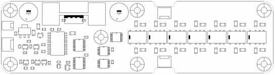
It is almost 3 years since I released V1 of this attenuator and 2 years since I mentioned making a V2 of it.
V2 will be ready in 3-4 weeks, I am done doing the layout, just need to make the Gerbers, order PCB's, components, assemble a board and do some testing.
The design is very close to the original but with some necessary changes/improvements.
Some info :
127 x 0.6 dB steps for an attenuation range of 0 to -76dB
10K impedance.
Onboard regulators, 5VDC for the digital logic and 5VDC for the relays.
A size of 150mm x 40mm.
Made a few improvements to the digital logic and a few bug fixes.
When I have more to show a new thread will be opened.
Very good news! I'm still very satisfied with my V1!
Will the V2 support balanced operation? Ideally with a single pot for two boards?
Will the V2 support balanced operation? Ideally with a single pot for two boards?
I still don't fully understand why a single potentiometer couldn't control two (or more) boards. Referring to the schematic attached to post #1, the control potentiometer (say 10k) is connected across the attachment points X3-3 and X3-1, with the wiper connected at X3-2. Point X3-2 goes into VIN+ of IC1.
Why can't a second attenuator board have a 10k resistor from X3-3 to X3-1, and have X3-2 connected to X3-2 of the first board (wiper of the only pot)? If interaction of the VIN+ pins of two boards would be a problem, could a DC coupled unity gain buffer isolate the pins?
Why can't a second attenuator board have a 10k resistor from X3-3 to X3-1, and have X3-2 connected to X3-2 of the first board (wiper of the only pot)? If interaction of the VIN+ pins of two boards would be a problem, could a DC coupled unity gain buffer isolate the pins?
I still don't fully understand why a single potentiometer couldn't control two (or more) boards. Referring to the schematic attached to post #1, the control potentiometer (say 10k) is connected across the attachment points X3-3 and X3-1, with the wiper connected at X3-2. Point X3-2 goes into VIN+ of IC1.
Why can't a second attenuator board have a 10k resistor from X3-3 to X3-1, and have X3-2 connected to X3-2 of the first board (wiper of the only pot)? If interaction of the VIN+ pins of two boards would be a problem, could a DC coupled unity gain buffer isolate the pins?
The way this board works, that is sadly not an option.
It could be done but require adding a 9 pin connector to the board and then have a smaller addon board that connects to the master board.
However, since I am limited to a size of 150 mm x 40 mm I really dont have the extra space for it, though I guess I could look into it some more. I had a colleague at work who asked me to make it possible to use it for balanced signals so you are not the only one that wants that option. 🙂
I also would like to see a balanced version.
/S.
/S.
The way this board works, that is sadly not an option.
It could be done but require adding a 9 pin connector to the board and then have a smaller addon board that connects to the master board.
However, since I am limited to a size of 150 mm x 40 mm I really dont have the extra space for it, though I guess I could look into it some more. I had a colleague at work who asked me to make it possible to use it for balanced signals so you are not the only one that wants that option. 🙂
It is not going to happen, V2 will be singleended only.
I just do not see the value in it. Balanced signals is great between equipment but internally I believe that singleended is the way to go.
I agree.It is not going to happen, V2 will be singleended only.
I just do not see the value in it. Balanced signals is great between equipment but internally I believe that singleended is the way to go.
Balanced impedance connections are for the connections
It's the connection that needs the balanced impedances, that reject the interference.
Yesterday I was finally done with the layout.
Gerbers were created and PCBs ordered.
V1 PCB's had a HASL surface finish, V2 will be ENIG instead. 🙂
Gerbers were created and PCBs ordered.
V1 PCB's had a HASL surface finish, V2 will be ENIG instead. 🙂
Any progress?
Yes, the PCB's have arrived in my country yesterday, now I am waiting for them to arrive at my adress.
So there is some progress being made, albeit slowly and totally out of my hands. 🙂
Yes, the PCB's have arrived in my country yesterday, now I am waiting for them to arrive at my adress.
So there is some progress being made, albeit slowly and totally out of my hands. 🙂
PCB's were delivered yesterday, components will be ordered tomorrow.
I should have something to show sometime next week. 🙂
PCB's were delivered yesterday, components will be ordered tomorrow.
I should have something to show sometime next week. 🙂
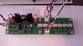
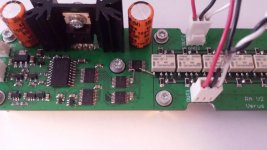
It took some time but it is finally done!
It had just 1 problem first time I turned it on, it didn't bloody work. 😕
However the ULN2003 relay driver was getting pretty hot and there was 5 Volt at all outputs with the volume turned all the way down or all the way up. Turned out I made a schematic error, the ULN2003 Relay Driver should have PIN 8 GND connected to GND and PIN 9 COMMON connected 5V used for the relays. I had them switched on the schematic and therefore also on the board.
Luckily I just had to lift the PIN 8 GND and PIN 9 Common legs and sold them to the right connections, by using 2 clipped off and correctly bent legs from a LED and it worked. 😀
Anyway now that it works I can safely say everything I wanted to achieve with V2 has been achieved. V1 could be a little unstable at times, relays going into constant chatter mode requiring you to turn the pot a little.
The changes I made in V2 removes this error mode, if it does happen and the POT voltage is just between 2 steps the relays stop changing state after between 1 or 2 relay cycles, that is 10 ms and 20 ms respectively and then it will stay 100% stable until you touch the volume control again.
All in all, I am very happy. 😎
Last edited:
Did you consider right - left balance?
As it is now, with 0.1% resistors in the attenuator, channels should be better matched than 0.1dB at ALL volume levels.
EDIT : Just calculated it, the channels should be better matched than 0.02dB which should be plenty. 🙂
Last edited:
- Status
- Not open for further replies.
- Home
- Source & Line
- Analog Line Level
- Pop/click free HW-based relay attenuator