If you read further in the thread the expert (read Jocko) did not agree.Thanks! According to this post in that thread the following input section is recommended:
You might also try Jocko's buffered spdif input. I don't remember where it was shown first but this is the same: https://www.diyaudio.com/community/threads/buffer-spdif-input-stage-for-ess9018.208452/post-2939451
I'm still really impressed with your ambition!👍
But also still having trouble understanding why, for example, in your post 80, you find it reasonable to eliminate 9 components! Could it be that you have an extremely dim view of the competence of the design engineer? I've succumbed to the urge a few times (to excise parts from a wiser person's design) over the years, and rarely did it end up with no teeth marks in my backside. 😉
You're so good at turning out beautiful PCB's and riveting simulations in mere hours . . Why not just accept the possibility that those parts were designed-in by someone that knew things about electronics that you don't. Maybe sound engineering practice was even employed -- perhaps yielding performance or reliability improvements, or to maintain performance across component tolerances, or interconnect vagaries, or over the full consumer temperature range . .
Layout the board, order the parts, build it when they come in, AND THEN ask for help if it doesn't meet expectations. It could be much more fruitful in terms of knowledge gained. And you would spare the time and expertise of the many fine minds contributing to this site, even though it would be at a somewhat higher cost to you.
Just my 2¢ . .
Cheers
Last edited:
But also still having trouble understanding why, for example, in your post 80, you find it reasonable to eliminate 9 components!
The schematic with the additional components I put together after someone suggested the more complex input section. The one I currently use does have less parts... Also I have seen that Pavouk uses an even simpler input section in his DIR9001 based SPDIF project - BTW he also has the 75R on the secondary of the pulse transformer...
I can't always distinguish if a diagram shown on the forum was created by a diyer or a design engineer - but if I can I always trust 😎Could it be that you have an extremely dim view of the competence of the design engineer?
Layout the board, order the parts, build it when they come in, AND THEN ask for help if it doesn't meet expectations.
Isn't that what I did...? I made the first PCB based on my simulations. That PCB had lot's of options (jumpers, etc.), I tested many things, and now want to make a "final" version. The input section works, the only remaining question is about the clicks/pops when switching inputs: but I think these must be from somewhere else as they appear even while the PMD100 is muted. If I get no input on that I will proceed with my second (and last) PCB...
I gather you did not read the thread I linked. If you have 75R on both primary and secondary of the transformer the impedance seen by the SPDIF connector is not 75 ohms. But it will most probably work anyhow. The proper termination is important if you want to minimize reflections and EMI. And it requires that you use a proper 75 ohm BNC connector (not RCA).The schematic with the additional components I put together after someone suggested the more complex input section. The one I currently use does have less parts... Also I have seen that Pavouk uses an even simpler input section in his DIR9001 based SPDIF project - BTW he also has the 75R on the secondary of the pulse transformer...
I gather you did not read the thread I linked. If you have 75R on both primary and secondary of the transformer the impedance seen by the SPDIF connector is not 75 ohms. But it will most probably work anyhow. The proper termination is important if you want to minimize reflections and EMI. And it requires that you use a proper 75 ohm BNC connector (not RCA).
I did read, and hence I was able to draw the schematic with the (corrected) values suggested for the last version of the input circuit... So it seems you did not really look at my diagram 😉
Like I already posted that is not the correct input circuit. Member rlim got it wrong.I did read, and hence I was able to draw the schematic with the (corrected) values suggested for the last version of the input circuit... So it seems you did not really look at my diagram 😉
OK, I tried again to gather all information of that thread, here are the results. First the output circuit as discussed in #42 of that thread:
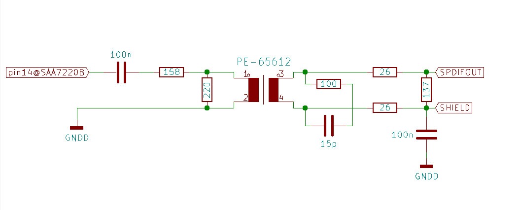
...he said, so do I have to worry about blowing the RX?
Here is the input circuit from #58:
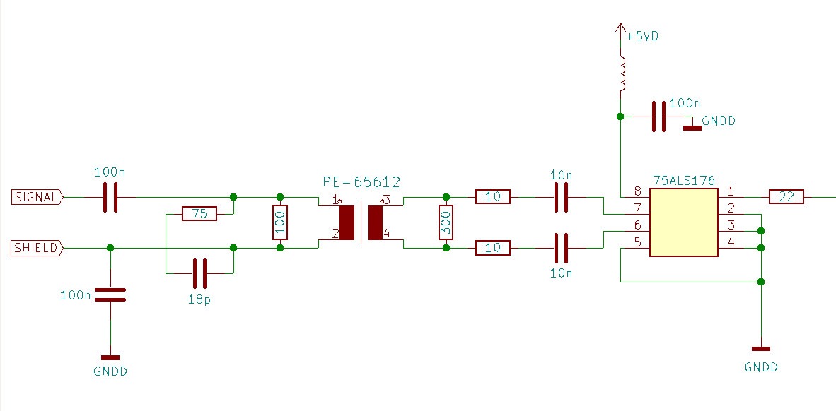
I guess it's also kind of active as I have the 75ALS176. Did I get it right this time...?
I did not calculate the pad values, but it can be a little bit high without having to worry about blowing the protecton diodes in the RX front end, or worse, creating tons of EMI.
...he said, so do I have to worry about blowing the RX?
Here is the input circuit from #58:
I guess it's also kind of active as I have the 75ALS176. Did I get it right this time...?
Since DIR9001 has single-ended spdif input 75ALS176 seems overkill. You could replace it with a single 74HCU04 (or 74HC1GU04).I guess it's also kind of active as I have the 75ALS176. Did I get it right this time...?
Since DIR9001 has single-ended spdif input 75ALS176 seems overkill. You could replace it with a single 74HCU04 (or 74HC1GU04).
I have some low Vpp sources, the 75ALS176 works well with them...
While 75ALS176 may work the approach normally taken is to treat SPDIF as what is is (an analog signal) and use 74HCU04 as a linear amplifier. This was the approach in the old threads I linked and is still the recommendation by e.g. ESS for their DACs.
the approach normally taken is to treat SPDIF as what is is (an analog signal) and use 74HCU04 as a linear amplifier.
That puzzles me: I thought SPDIF was a digital signal, and the 74HCU04 a digital inverter, and now I read SPDIF is analog and the logic gate is a linear amplifier...?? Also if SPDIF has 1Vpp how can the HCU04 with it's min VIH of 1.7V detect the signal at all...?
Last edited:
SPDIF is analog signal carrying digital information. Regarding using HCU04 as linear amplifier you can read more from e.g. here: http://melbmcu.weebly.com/cmos-gate-as-analogue-amplifier.html
BTW SPDIF is only 0.6Vp-p.
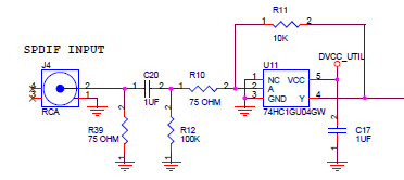
As an example here is the SPDIF input from ES9038Q2M evaluation board.
BTW SPDIF is only 0.6Vp-p.
As an example here is the SPDIF input from ES9038Q2M evaluation board.
Last edited:
The second inverter stage may not be needed and I would anyhow use single gate inverters. 75ALS176 costs way more than all the components put together (excl. transformer).
Thanks a lot for the help, I made the layout and ordered the new PCB. I will report once I got it working...
I got the PCB and the parts, build everything up. All the reclocking / delay etc. works fine, but there is a problem with clock transmission, I get reflection and/or crosstalk. It goes away if I touch the inverted XTI line with my finger (or with the scope). Here is the diagram:
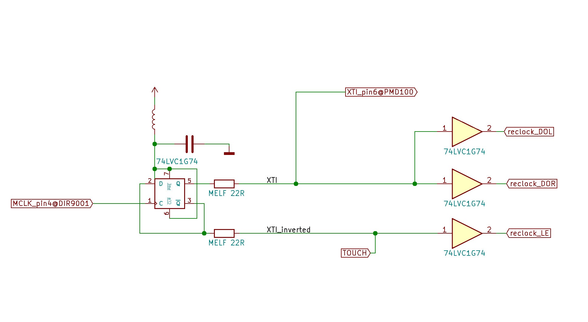
The 3 gates on the right side work as intended (they are the same circuits as the older PCB). The flip flop on the left side devides the incoming clock signal by 2. If I probe the XTI-line I get the following signal:
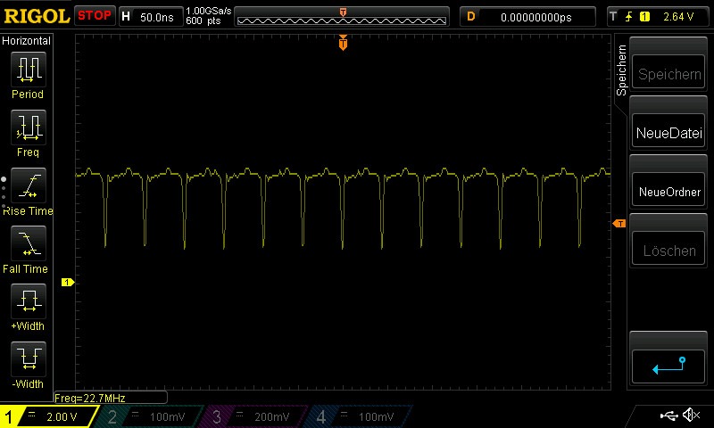
Only if I touch the inverted XTI line I get this signal:
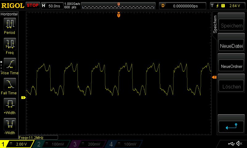
Also not really beatiful but at least it works and I get clean sound from the DAC. I don't have a clue about high frequency transmission, so I tried to read on this, but didn't really understand what's going on. I think I have to re-arrange the termination resistors...? Please help!
The 3 gates on the right side work as intended (they are the same circuits as the older PCB). The flip flop on the left side devides the incoming clock signal by 2. If I probe the XTI-line I get the following signal:
Only if I touch the inverted XTI line I get this signal:
Also not really beatiful but at least it works and I get clean sound from the DAC. I don't have a clue about high frequency transmission, so I tried to read on this, but didn't really understand what's going on. I think I have to re-arrange the termination resistors...? Please help!
All sorted now. There was a minor mis match of logic levels between some of the ICs.
I had to revert to my working version of the input section - all the talk about active spdif etc. was just waste of time.
Twisted DEM cables resulted in horrible distortion, so beware. It would be good to connect the outer foil of the blocking caps to the high impedance side though. I use styrenes, C0Gs and X7Rs did not work.
I use the mcu to control the output relay of the Arcam, now I have clean mute at power on and input selection. As the relay is fed from the -15V supply I used an opto coupler to switch it.
Finally I can confirm that my reclocked circuit as of #77 sounds even better. Well worth the effort!
Do you mean that the circuit with unbuffered inverter (as in post #92) did not work? That would be very strange since even the DIR9001 evaluation board uses such setup for coax input.I had to revert to my working version of the input section - all the talk about active spdif etc. was just waste of time.
The DIR9001 eval board does not use LVC logic, the topology is slightly different, and the front end is very different (no transformer etc).
The 75ALS allows me to spare even one of the 125 buffers as it has an enable pin. Or use a 26C32 for multiple inputs...
The 75ALS allows me to spare even one of the 125 buffers as it has an enable pin. Or use a 26C32 for multiple inputs...
Last edited:
The transformer or logic family is not relevant for the operation and besides DIR9001 evaluation board uses 74LVU04. But of course you canuse 75ALS if it suits you. I recommend to check the jitter with e.g. JTEST.
- Home
- Source & Line
- Digital Line Level
- PMD100 to TDA1541 in smultaneous mode