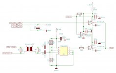
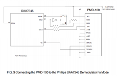
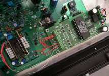
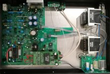
Yes, I designed a small PCB with a complete interface for the TDA1541A while I am waiting for a new chip to arrive... See attached pictures: transformer isolated coax and toslink SPDIF inputs can be switched, DIR9001 receiver, PMD100 digital filter (compatible with SM5813/DF1700), and glue logic with various possibilities to test out which one works best... I will report how things go on!
Attachments


Wait a bit with PCBs... When You recklock data line (or other) with just one FF output will be 1/2 delayed for 1/2 period of MCK that recklocking data. Try to put in series another FF to meet the output for round one period of MCK and rising/falling edges matching. And to avoid metastabile events...
Hi BramYou cannot clock 20 bits into the TDA1541.
and use complementary offset binary
I had succes today with DF1700 running 8xOS on TDA1541 and tda1541A in Sim_mode
https://www.bramjacobse.nl/wordpress/?p=8972
Could You post the schematic for this interface You used in the link?
That's what is intended: delay of DATA lines half a cycle to align with falling edges of BCK. How can metastable events occur?Wait a bit with PCBs... When You recklock data line (or other) with just one FF output will be 1/2 delayed for 1/2 period of MCK that recklocking data. Try to put in series another FF to meet the output for round one period of MCK and rising/falling edges matching. And to avoid metastabile events...
Hi Bram
Could You post the schematic for this interface You used in the link?
Sorry idont have a schematic, i used some datasheets and the flip-flop from the nakamiche schematic.
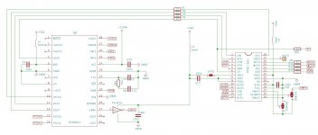
I'm now using a WM8804 a spdif recciever --> DF1700 --> TDA1541(a)
http://www-classes.usc.edu/engr/ee-s/552/coursematerials/ee552-G1.pdfThat's what is intended: delay of DATA lines half a cycle to align with falling edges of BCK. How can metastable events occur?
Does it mean a lot without sch? But OK...Sorry idont have a schematic, i used some datasheets and the flip-flop from the nakamiche schematic.
I'm now using a WM8804 a spdif recciever --> DF1700 --> TDA1541(a)
There is a Guido T circuit from another forum. (At the moment link is not working, and site is not available?..)

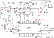
It is little different from I2S input interface n the PMD100 datasheet. Without inverter for CLK F-F input.
.
Note that Deglitch pin output from PMD100 can be used as source for the DEM pins @ TDA1541A.
And Format is in COB so no need to invert MSB. That is huge advantage.
.
But stopped clock would be important.
.
Note that Deglitch pin output from PMD100 can be used as source for the DEM pins @ TDA1541A.
And Format is in COB so no need to invert MSB. That is huge advantage.
.
But stopped clock would be important.
Attachments
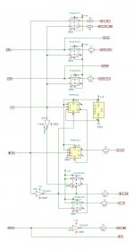
another interface solutions
https://tinyurl.com/y8fjayywand with a wider LE
https://tinyurl.com/y9nasu6chttps://tinyurl.com/y8zdsepc
https://tinyurl.com/y8fjayywand with a wider LE
https://tinyurl.com/y9nasu6chttps://tinyurl.com/y8zdsepc
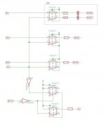
The PCB works: SPDIF coax / toslink switchable. TDA1541A sounds wonderful from PMD100. I tried a couple of configurations, the attached circuit worked and sounded best. Questions remain about the coax input circuit:

Are R19 and R20 really needed? What about C32 and R16, R17, R21, R22...? Also, should I add reclocking for BCK? If yes I need to again delay the data lines, here a simulation of a reclock of all lines - what do you think?
Are R19 and R20 really needed? What about C32 and R16, R17, R21, R22...? Also, should I add reclocking for BCK? If yes I need to again delay the data lines, here a simulation of a reclock of all lines - what do you think?
Attachments
Thanks for sharing infos
You can not recklock BCK with 11.xxxMHz since the BCK is alreadu have the same F (11.xxxMHz).
For recklocking BCK from PMD100 You need 2x higher Master clock.
.
I thik that some mistkes are in the sim page. BCK F is not 352.8KHz but 11.xxMHz.
And data ines F is 1/2 of BCK.
Should be like this
https://tinyurl.com/y7re3ohqall lines are in phase and all of the periods are 50%
But this is with MCK of 22.5792 MHz and PMD100 maybe could not accept this.
Ths is for the USB interfaces, most of them have 22.xxx/24.xxx MHz MCKs, but could be divide by 2 with some J-FF
.
You already have some form of recklocking for data L/R. Just add one more FF after FF in each data R/L lines.
That will additionaly delay data lines for 1/2 period of clock F
.
Did You tried with DEM part?
How was preseted BCK phase in the PMD100 pin. Inverted BCK or not inverted?
Last edited:
Yes, the simulation has random frequencies and duty cycles, but I wanted to show delay in half steps, hence I used inverted and non-inverted clocks for the flipflops...
Yes, I considered a USB input as well, but for now I will keep it as it is and enjoy...
I intended 1/2 delay because inverted BCK seems to mess up the internal latch of the TDA1541A...
Yes, with and without... With was an improvement!
But this is with MCK of 22.5792 MHz and PMD100 maybe could not accept this.
Ths is for the USB interfaces, most of them have 22.xxx/24.xxx MHz MCKs, but could be divide by 2 with some J-FF
Yes, I considered a USB input as well, but for now I will keep it as it is and enjoy...
You already have some form of recklocking for data L/R. Just add one more FF after FF in each data R/L lines.
That will additionaly delay data lines for 1/2 period of clock F
I intended 1/2 delay because inverted BCK seems to mess up the internal latch of the TDA1541A...
Did You tried with DEM part?
Yes, with and without... With was an improvement!
Could You please post some scope measurements of the lines? With for instnce 2-3 words long.
and settings for PMD100 about BCK polarity pin?
and settings for PMD100 about BCK polarity pin?
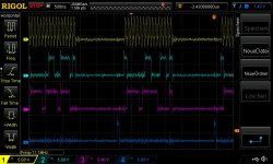
Attached my scope shots: yellow = BCK, green = DATA_L, red = DATA_R, blue = LE. Circuit is shown in #54.
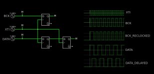
As for reclocking BCK: I simplified the my simulation. The screenshot shows that the timing between BCK and DATA is correct (I could take a 512x MCLK from the DIR9001 and divide it before feeding it to the PMD100), what do you think?
As for reclocking BCK: I simplified the my simulation. The screenshot shows that the timing between BCK and DATA is correct (I could take a 512x MCLK from the DIR9001 and divide it before feeding it to the PMD100), what do you think?
Attachments

wow fast work 🙂
I think that You could divide 512x MCLK from the DIR9001 to 256X for XTI PMD100
with J-FF You can choose which polarity is better and maybe You can remove one inverter since divided MCK can have inverted out?
https://tinyurl.com/y7l56d7r.
Probably delay for 1/2 11.xxxMHz will hot change anything. As long as LE stayed like it is, as maybe most important line
.
About SPDIF input consult topologies and value of load resisitors for ballanced input transformers. Ususaly they have circuits labeled as proffersional.
- Home
- Source & Line
- Digital Line Level
- PMD100 to TDA1541 in smultaneous mode