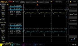
Update: I think I finally got rid of the problem I mentioned in #108 😎
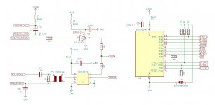
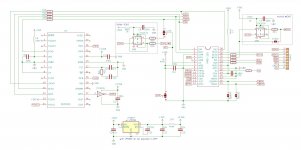
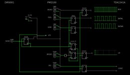
The solution was to attenuate the signals to the TDA1541A: I added a 2V2 regulator which feeds the gluelogic, so the signals to the TDA1541A only have 2V2. I also reclocked BCK (in order to get it down to 2V2) and added the Grundig DEM circuit (plus the possibility tu run the PMD100 in software mode should I want to). Corrected schematics are attached.
I also tried a couple of bit decoupling caps at the TDA1541A. I went for 14 Kemet SMR 220nF caps plus 4 Panasonic ECHU 220nF under the PCB to get the original values Arcam used. As the DEM cap I liked a 680p WIMA FPK2. BTW I don't think active DEM clocking is really better, it's just different.
The updated simulation of the modified gluelogic can switch between 4x and 8x oversampling!
Attachments

Last edited:
That's very clever! I'd've never thought of that! 😏
Do we know that it's the 2V2 voltage swing and not the small additional delays imposed by operating the parts at the lower voltage? Especially since more than one logic family is involved . . each would get slower at a different rate . .
Still, an excellent achievement ! ! And what an undertaking -- great stuff -- thanks for doing this !
Cheers

Many thanks for your kind words!
I don't know if the small delays play a role, but AUP logic could be used to get the delays even shorter. At least I made sure the TDA1541A "sees" the same kind of drivers from all it's input pins (which was not the case in the previous version).
One question remains in regard to the Grundig DEM circuit which now also sees a 2V2 signal - should I revert that back to 3V3...?
Good news 🙂 jpk73
Yes it was a topic long time ago about input levels for TDA1541A. And some solutions for line attenuators. I cant find the link right now...
In the datasheet noted that
digital inputs LOW VI = 0.8 V
digital inputs HIGH VI = 2.0 V
.
About DEM level try to consult article from PHI book? I think we have a post of that in the topic before?
Wow!Update: I think I finally got rid of the problem I mentioned in #108 😎
The solution was to attenuate the signals to the TDA1541A: I added a 2V2 regulator which feeds the gluelogic, so the signals to the TDA1541A only have 2V2. I also reclocked BCK (in order to get it down to 2V2) and added the Grundig DEM circuit (plus the possibility tu run the PMD100 in software mode should I want to). Corrected schematics are attached.
I also tried a couple of bit decoupling caps at the TDA1541A. I went for 14 Kemet SMR 220nF caps plus 4 Panasonic ECHU 220nF under the PCB to get the original values Arcam used. As the DEM cap I liked a 680p WIMA FPK2. BTW I don't think active DEM clocking is really better, it's just different.
The updated simulation of the modified gluelogic can switch between 4x and 8x oversampling!
Awesome work!
And how about the improvement in the way your Black Box usually sounds?
Have fun!
https://www.diyaudio.com/community/threads/pmd100-to-tda1541-in-smultaneous-mode.382655/post-6964002
link to the PHI book page about "Grundig" DEM 🙂
it is about 2.5V-5V TTL input level to DEM circuit.
link to the PHI book page about "Grundig" DEM 🙂
it is about 2.5V-5V TTL input level to DEM circuit.
Wow!
Awesome work!
And how about the improvement in the way your Black Box usually sounds?
Have fun!
I don't know how the stock Arcam sounds - have forgotten it, also it was not recapped back than, and I listened to it with so many variations of that PMD100 adapter. All I can say it sounds really good now!
https://www.diyaudio.com/community/threads/pmd100-to-tda1541-in-smultaneous-mode.382655/post-6964002
link to the PHI book page about "Grundig" DEM 🙂
it is about 2.5V-5V TTL input level to DEM circuit.
Thanks! There is a voltage divider, so HIGH=5V would make 1.25V at the entry of the DEM circuit. The Grundig CD9009 shows no divider, just a series 2k2 resistor, fed from the CXD1244S with HIGH=5V. So am I right to assume that anything between 1.25 and 5V should work well...?
I think so. But You can try some values to compare if You want. link for att. issues on TDA1541A https://www.diyaudio.com/community/...ate-nos-dac-using-tda1541a.79452/post-5490534So am I right to assume that anything between 1.25 and 5V should work well
there was more about this in some earlier topics but I couldn't find these links... 🙁
Thanks! But I don't like attenuation by resistors or diodes, better have the output logic ICs run at lower voltages...
No it is not better. Better to have constant load paired with input capacitance. Maybe just to use bridged T network against L-pad.
Other thing is common for lowering voltage IC and/or att. is that we lowering Hi, positive value only. Other Lo value remains around GND or 0V.
I will try to find one simple network with JFET, diode and R, that can be tuned to fit Hi-Lo region.
Other thing is common for lowering voltage IC and/or att. is that we lowering Hi, positive value only. Other Lo value remains around GND or 0V.
I will try to find one simple network with JFET, diode and R, that can be tuned to fit Hi-Lo region.
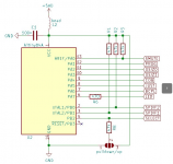
Yes, Arduino is the simplest. Here is the code (you need to include my library from here):
This code is for the switch on the front panel of the Arcam. The LED output is connected to the mute relay. If you use push buttons you need to use button.clicked(), see this example.
BTW I would be keen to see a working code example for the software mode of the PMD100!
C#:
// for ATtiny84
// pin mapping clockwise
// set clock to 4MHz internal

#include <avr/sleep.h>
#include <debouncetm.h>

#define MUTE           0  // MUTE (HIGH = muted)
#define PROG           1  // HARDWARE MODE: LOW
#define OSIZ0          2  // HARDWARE MODE: LOW
#define OSIZ1          3  // HARDWARE MODE: LOW
#define COB            4  // HARDWARE MODE: LOW
#define JUST           5  // HARDWARE MODE: LOW
#define BCPL           6  // HARDWARE MODE: LOW
#define LED            7  // LED (active HIGH)
#define TOSLINK       10  // TOSLINK (active LOW with 74LVC125, active HIGH with 74LVC126)
#define COAX           9  // COAX (active LOW)
#define buttonpin      8  // button pin (HIGH = TOSLINK)

#define samplerate    0.75  // poll interval for update() in msec (a safe starting point would be samplerate = 0.1 * bounce-duration in msec)
#define longpress     0.90  // longpress duration in sec
#define doubleclick   0.50  // doubleclick window in sec
Button button(buttonpin, INPUT, HIGH, samplerate, longpress, doubleclick);  // specify pin, pinMode, polarity, samplerate, longpress duration, doubleclick window

elapsedMillis sleep_timer;
unsigned int sleep_interval = 500;   // mute ramp down takes 260ms, so 300 is a good value here

void setup() {
  delay(1000);
  pinMode(COAX, OUTPUT);
  pinMode(TOSLINK, OUTPUT);
  pinMode(MUTE, OUTPUT);
  pinMode(LED, OUTPUT);

  pinMode(PROG, OUTPUT);
  pinMode(OSIZ0, OUTPUT);
  pinMode(OSIZ1, OUTPUT);
  pinMode(COB, OUTPUT);
  pinMode(JUST, OUTPUT);
  pinMode(BCPL, OUTPUT);

  digitalWrite(LED, LOW);
  digitalWrite(OSIZ0, LOW);
  digitalWrite(OSIZ1, LOW);
  digitalWrite(COB, LOW);
  digitalWrite(JUST, LOW);
  digitalWrite(BCPL, LOW);
  delay(100);
  digitalWrite(PROG, LOW);
  digitalWrite(MUTE, HIGH);
  digitalWrite(COAX, HIGH);
  digitalWrite(TOSLINK, LOW);

  delay(3000);

  if (!digitalRead(buttonpin)) {
    digitalWrite(COAX, LOW);
    delay(50);
    digitalWrite(LED, HIGH);
    delay(300);
    digitalWrite(MUTE, LOW);
    delay(300);
  }
  sleep_timer = 0;
}

void loop() {
  button.update();
  if (button.pressed()) {select_toslink();}
  if (button.released()) {select_coax();}
  if (sleep_timer > sleep_interval) {gotoSleep();}
}

void select_toslink() {
  digitalWrite(MUTE, HIGH);
  delay(300);
  digitalWrite(LED, LOW);
  delay(200);
  digitalWrite(COAX, HIGH);
  delay(50);
  digitalWrite(TOSLINK, HIGH);
  delay(50);
  digitalWrite(LED, HIGH);
  delay(300);
  digitalWrite(MUTE, LOW);
  delay(300);
  sleep_timer = 0;
}

void select_coax() {
  digitalWrite(MUTE, HIGH);
  delay(300);
  digitalWrite(LED, LOW);
  delay(200);
  digitalWrite(TOSLINK, LOW);
  delay(50);
  digitalWrite(COAX, LOW);
  delay(50);
  digitalWrite(LED, HIGH);
  delay(300);
  digitalWrite(MUTE, LOW);
  delay(300);
  sleep_timer = 0;
}

void gotoSleep() {
  GIMSK |= _BV(PCIE0);
  GIMSK |= _BV(PCIE1);
  PCMSK1 |= _BV(PCINT10);                 // use PB2 as interrupt pin
  // PCMSK0 |= _BV(PCINT4);               // use PA4 as interrupt pin
  ADCSRA &= ~_BV(ADEN);                   // ADC off
  set_sleep_mode(SLEEP_MODE_PWR_DOWN);    // replaces above statement
  sleep_enable();                         // sets the sleep enable bit in the MCUCR register (SE BIT)
  sleep_cpu();                            // sleep
  sleep_disable();                        // clear SE bit
  PCMSK1 &= ~_BV(PCINT10);                // turn off PB2 as interrupt pin
  // PCMSK0 &= ~_BV(PCINT4);              // turn off PA4 as interrupt pin
  ADCSRA |= _BV(ADEN);                    // ADC on
  sleep_timer = 0;
}

// ISR(PCINT0_vect) {sleep_timer = 0;}
ISR(PCINT1_vect) {sleep_timer = 0;}
This code is for the switch on the front panel of the Arcam. The LED output is connected to the mute relay. If you use push buttons you need to use button.clicked(), see this example.
BTW I would be keen to see a working code example for the software mode of the PMD100!
Last edited:
Look for the PMD100 Microprocessor Control Application Note. It has assembler code written for the MC68HC705.BTW I would be keen to see a working code example for the software mode of the PMD100!
I saw this app note once long time before. Maybe I can dig and post this PDF from some old HD?
.
Can we use micro-controller from PMD200 to control PMD100 in soft mode maybe? With code adopted for PMD100...
https://www.diyaudio.com/community/...th-pmd-200-into-stand-alone-dac.374577/page-9
.
Can we use micro-controller from PMD200 to control PMD100 in soft mode maybe? With code adopted for PMD100...
https://www.diyaudio.com/community/...th-pmd-200-into-stand-alone-dac.374577/page-9
I saw this app note once long time before. Maybe I can dig and post this PDF from some old HD?
.
Can we use micro-controller from PMD200 to control PMD100 in soft mode maybe? With code adopted for PMD100...
https://www.diyaudio.com/community/...th-pmd-200-into-stand-alone-dac.374577/page-9
Yes, it's my code... Can run on Arduino or whatever. But the PMD100 uses a different control "language". If I know how it works I can generated the same flexible solution as I did for the PMD200.
I cant understand why it is so complicated for PMD100?
.
I think that can be achieved even with glue logic ICS
MDT line = 24 bit data word register can be set manualy bu switches in the cascode of 3 x PISO (HC165 or sim)
MS1, MS2, MS3 = contrlol lines setiing the reception of data serial word in internal register.
-MEN = sort of stopped clock line with max F of about 33.3MHz period, (2 x 15ns min. time per cycle) as a window for word 24bit word register preset.
so we can use some master clock 22. 24. base?
.
This is for Mode Control register control, without additional option of Attenuation control that might be not necessary?
.
one first impulse can be generated from some 555 time cirvuit to control the logic MS1, MS2 and MS3 for managing 24bit serial data word
.
But it is hard to believe that is not possible to generate 5 digital lines in specific order and relation with arduino?
.
.
I think that can be achieved even with glue logic ICS
MDT line = 24 bit data word register can be set manualy bu switches in the cascode of 3 x PISO (HC165 or sim)
MS1, MS2, MS3 = contrlol lines setiing the reception of data serial word in internal register.
-MEN = sort of stopped clock line with max F of about 33.3MHz period, (2 x 15ns min. time per cycle) as a window for word 24bit word register preset.
so we can use some master clock 22. 24. base?
.
This is for Mode Control register control, without additional option of Attenuation control that might be not necessary?
.
one first impulse can be generated from some 555 time cirvuit to control the logic MS1, MS2 and MS3 for managing 24bit serial data word
.
But it is hard to believe that is not possible to generate 5 digital lines in specific order and relation with arduino?
.
Last edited:
Did I say it's hard to code...? 😉
Of course it's the best solution, hence I included the ATtiny with enough pins connected to the PMD... Just don't want to spend time on it if there exist working solutions which must surely be the case...
Of course it's the best solution, hence I included the ATtiny with enough pins connected to the PMD... Just don't want to spend time on it if there exist working solutions which must surely be the case...
The main issue is to use the PMD100 in 2X OS mode only option in program mode. And maybe some DG positions option
ATtiny managing control only in stand alone mode. Emulating manual switches. With preset of 8 X OS mode.
.
But did You tried register control for PMD100 with working PMD200 module maybe?
ATtiny managing control only in stand alone mode. Emulating manual switches. With preset of 8 X OS mode.
.
But did You tried register control for PMD100 with working PMD200 module maybe?
- Home
- Source & Line
- Digital Line Level
- PMD100 to TDA1541 in smultaneous mode