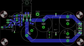
You dont need to worry too much about the connector side. You can have 150mil track width in there.
But you need to worry about the IC side.
I think your program allowes different track widths at different parts of it? Or you can use fills. Cant help you with eagle. I use different program.
But the area between C7/8 and the negative power track must be filled with copper.
Same thing with the area on top of the C3/7 and positive power track, fill it with copper - some how.
For example, use two narrower tracks from the IC to the capacitors and afterwards fill the empty area between those. One track from lets say the pin 3 to the C13, as you have it now. And then an other from the C8 to the C13. Then fill the area between... I do not know how your program works, so you need to experiment.
Anyhow, the ground tracks. Remowe them. You can leave the nest. But no ground tracks yet.
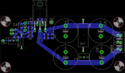
C10, move it down to the middle of the PCB, into the center of the cap bank.
R8, lay it down. Use a 2W type. C10 can be a 63v type, so you can get closer to it with the resistor. 63V 100nF MKT is 2.5mm thick.
Also, no need to find the specific blade terminal. Just put the pads there. Pad size 3.5mm, hole size 1.8mm and distance 200mils.
But you need to worry about the IC side.
I think your program allowes different track widths at different parts of it? Or you can use fills. Cant help you with eagle. I use different program.
But the area between C7/8 and the negative power track must be filled with copper.
Same thing with the area on top of the C3/7 and positive power track, fill it with copper - some how.
For example, use two narrower tracks from the IC to the capacitors and afterwards fill the empty area between those. One track from lets say the pin 3 to the C13, as you have it now. And then an other from the C8 to the C13. Then fill the area between... I do not know how your program works, so you need to experiment.
Anyhow, the ground tracks. Remowe them. You can leave the nest. But no ground tracks yet.
C10, move it down to the middle of the PCB, into the center of the cap bank.
R8, lay it down. Use a 2W type. C10 can be a 63v type, so you can get closer to it with the resistor. 63V 100nF MKT is 2.5mm thick.
Also, no need to find the specific blade terminal. Just put the pads there. Pad size 3.5mm, hole size 1.8mm and distance 200mils.
Now it looks quite bad actually...
What I have in mind with the power tracks, is attached.
Lets try the following:
Move C13 to the left. We have a lot of unused space there. Move it about 200mils to begin with... and turn it to a 45degree angle.
Move C12 down as much as needed to get a straight track from it to the IC.
Now we have also made new space for C10. Turn it vertically between R8 and C13. Top pin is the GND.
You should now have more space also for the speaker connector.
Attachments
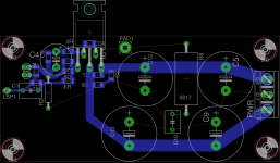
Could manage it without rotating the cap. Let me know if i still need to.
last mile to the chip is still 100 mils. rest of the power tracks are 150. If I make it all 150 mils, the c12 to pin5 tracks overshoots and touches pin3. If I dont take it all the way, it shows me pending nest.
last mile to the chip is still 100 mils. rest of the power tracks are 150. If I make it all 150 mils, the c12 to pin5 tracks overshoots and touches pin3. If I dont take it all the way, it shows me pending nest.
Attachments
C3,7,8 OK.
Turn C10 180degrees to have its GND upwards.
Turn C13 to the 45deg angle and move it to the left as much that you can have a straight connection from it to the IC pin 3. Iwant to see how it looks. However, try keep the negative rail looking like it is now and having it where it is now, with the similar 45deg angle you have on it now.
Move C10 upwards closer to the C12 (and 13)...
Does your software allowe to run several tracks between components?
Lets say 3 50mill tracks to make 150mill track (or even wider)???
I want wider tracks between IC and the Caps...
🙂
Lets say 3 50mill tracks to make 150mill track (or even wider)???
I want wider tracks between IC and the Caps...
🙂

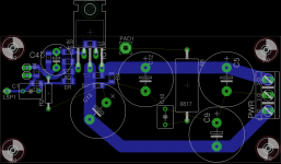
OK, we are getting there...
Move C13 upwards untill it almost hits the C12. Make its track to the IC about as long as the track from IC pin 5 to the C12.
Then from C13 leave the cap with 45degree track towards the C9 and then turn horizontally as you are in the right level.
Hopefully this made sense to you...???
Move C13 upwards untill it almost hits the C12. Make its track to the IC about as long as the track from IC pin 5 to the C12.
Then from C13 leave the cap with 45degree track towards the C9 and then turn horizontally as you are in the right level.
Hopefully this made sense to you...???
An SMD 805 will fit between the pins of the chipamp.
A 1206 can be soldered TO the pins of the chipamp.
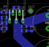
Move C7.
Have you checked for availability of smd 100V X7R ceramic?
A 1206 can be soldered TO the pins of the chipamp.
Move C7.
Have you checked for availability of smd 100V X7R ceramic?
You got it perfectly!
Now keep these 45degree angles on the bottom track what ever happens in the future...
Now we clean it up a bit.
Im still not quite happy with the Zobel, but maybe we just have to live with it.
However, move C5 closer to the board top edge, as close as you can get before it touches the mounting screw. Make the 45degree angles to the top track, first from the connector to the C5 and then down from C% in 45degrees untill you are in line with the C12...
Move C9 back in line with the C5 and upwards as close as possible. Remember to keep the 45deg angles on the bottom track.
Reduce PCB size from the bottom part...
Some fine tuning:
Input combo R3,4,5,C6; move it down just a little bit untill you are in line with C11 on the left (the ceramic that is).
If needed, move C7 in line with C6.
And move also C8 in line with the R3 if needed...
An SMD 805 will fit between the pins of the chipamp.
A 1206 can be soldered TO the pins of the chipamp.
Move C7.
Have you checked for availability of smd 100V X7R ceramic?
That could be possible to do...
Also, Andrew, thanks for the explanation of the faulth currents in R2. I need to further investigate that (find the discussions about it).
I have newer had a ground lift resistor between the two grounds in my amplifiers.
We need to add the diodes in there.
We could remove the C7 from the schematic. I would choose to solder A SMD1206-1210 directly to the IC pins in that case.
Or do you Andrew mean to solder the C7 between the pin rows (under pin 4 of the IC)???
Or do you Andrew mean to solder the C7 between the pin rows (under pin 4 of the IC)???
I did not have them for years.That could be possible to do...
Also, Andrew, thanks for the explanation of the faulth currents in R2. I need to further investigate that (find the discussions about it).
I have newer had a ground lift resistor between the two grounds in my amplifiers.
We need to add the diodes in there.
It was a casual observation of another Members sch that made me think "why does he show diodes there?"
A 806 fits between the pins 3 & 5. The pads are already there.
A 1208 spans between pins 3 & 5, above the PCB.
Do they make a 16xx size smd capacitor? That would sit nicely on the pins.
A 1208 spans between pins 3 & 5, above the PCB.
Do they make a 16xx size smd capacitor? That would sit nicely on the pins.
Do they make a 16xx size smd capacitor? That would sit nicely on the pins.
1812 ?
- Status
- Not open for further replies.
- Home
- Amplifiers
- Chip Amps
- please review this pcb design