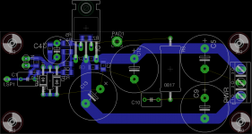
I have 603 cap betweens pins 1 & 2 of a 3886 and another between pins 2 and 4, spanning across pin3, but not touching.
I am using the Not Connected pin2 as a local Power Ground.
These two caps are soldered on just as the pins exit the plastic package. Very fiddly, but certainly possible. Seems to work.
Then a leaded 0.1" pitch cap between pins 2 & 5 to complete the HF local decoupling.
Pin2 then gets a trace connection to the MF decoupling electrolytics.
Unless I missunderstand something now, the PCB (including to decoupling) looks quite right to me???
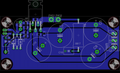
Anyhow, you could move the R8 upwards a bit, so that its top lead is in the middle of the free space between the (+) rail and PCB edge.
Maybe turn the C10 back to sideways(?).
Keep it close to R8 and C10. As far away from the (-) track as possible.
Remowe track from C8 to C3. Keep them in the ground net however... (We will do a magic trick in the end.)
We need the safety diodes around R2.
They require some space on both sides of the R2. One end will be connected to the audio ground (same way as the R2). Then connect with a net to the power ground (or R2 bottom end)...
Move the big elco C4 upwards just a tyny bit, so that you can fit a diode in parallel with the R2 on its right side.
There is no space for a leaded component on its left side, so we need to push (carefully) C1,C11,R1 and the input connector 100mils to the left. Make PCB 150mils wider to that direction also.
You can move input connector closer to the board edge if you want, but keep a minimum distance of abaut 150mils away from the edge.
Last edited:
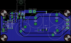
Looks, not too bad.
I might want to keep the R4/5 as close to the C6 as you had them previously.
You can also move C2 (ceramic) down in to the middle of C4.
I would still put an additional pad to the right of Pad1 (200mils appart) so that if one wants to use a Faston blade there...
Make connection from IC pin4 to the output Pad(s). Track width 150-200mils.
Make connection from Output pad(s) to the R8. Track width 50mils.
Make connection from C10 to R8, track width 50.
Drag the 45deg angle of the bottom power track from the power connector 150mils to the left, so that we have some more space between the mounting screw and the power track.
Push the magic button in your software for automatic ground fill/layer/pour, or what ever it is called in it...
Lets see what happens...
changes done.
Whats a good value for the supply caps..
4700uF 35V LowESR 105C
Supply rails close together... But its almost impossible on single sided design 🙁
We have the power side and the input side, and we will get a shield around the power side, so I do not find it to be a too big problem here.
But you are right, and we can not have everything with one layer only.
Also had a last minute idea:
If we turn Cap1 (+C11) vertically and move the input connector (+R1) down to the bottom side of the PCB, we can shrink the PCB a bit from the left. Also make use of the empty area on the bottom left corner.
Since we're reviewing PCBs....
How are the SMD components going to be soldered?
Manually or solder paste + Oven (toaster oven, SMD oven)?
Because if they'll be reflowed, the PCB layout on these SMD parts *might/probably/will* cause tombstoning problem - C8 and C3.
page 1.iii
http://metallicresources.com/documents/Tombstoning explained.pdf
If these will be manually soldered, then just ignore me.
apart from what you suggested, I also rotated c9 just like c13 and move the power connector a little bit up, this also raised the -ve power track a little bit upwards. this was to have a decent track width going from agnd to pgnd.
is 1n4007 good enough for the diodes.
i plan to do manual soldering only.
is 1n4007 good enough for the diodes.
i plan to do manual soldering only.
Attachments
Last edited:
4700uF 35V LowESR 105C
so there is no need for any caps in the psu? just feed the bridge rectfier output directly into this board. I can use a chassis mounted br in that case.
Component tombstoning is not a big problem in commercial PCB assembly, because you have to nail your processes down and cannot afford such problems. For home use you may have problems, good solder paste deposit is critical if you are using it (60% of reflow faults are due to paste stencilling problems). What ever way you use gluing the components down will help.
A quick note on point 'viii' from the above document...early infrared reflow machines were quite crude affairs with the board going through a curtain of heat (a temperature gradient across a 1210 cap or resistor is a bit frightening), often causing the solder on one end of a chip device to reflow before the other (tombstoning was more of a problem then Circa 1886-88). This also had other undesirable affects on many components, MLCCs being susceptible to cracking, ICs failing etc. Todays ovens are better controlled with pre-heat zones and proper profiling done for each assembly, and solder paste screening is a well studied and controlled operation.
Problems you may have with using a soldering iron is the device sticking to the iron, a hot air gun is a better option. Or use a small fan oven, the problem hear is controlling the temperature ramp up.
Another thing is to get your footprints correct, here the IPC-7351 documentation should be your guide...
A light version with a lot of the data can be found here:
PCBL - PCB Library Expert
There is more info such as the CAD library of the future...
http://www.dnu.no/arkiv1/The CAD Library of the Future.pdf
apart from what you suggested, I also rotated c9 just like c13 and move the power connector a little bit up, this also raised the -ve power track a little bit upwards. this was to have a decent track width going from agnd to pgnd.
is 1n4007 good enough for the diodes.
i plan to do manual soldering only.
You have rotated also C2 at the input circuit. Not good idea.
As you have C1 vertically (as suggested) you must also move input connector to the bottom edge of the PCB, otherwise you are creating a loop area there...
There is no need for a wide GND track at the bottom, but as you have space in there now, you could put a shield track between the negative rail and the ground track, or increase the distance between these two tracks, lets say to 50mils...
4007 is appropriate for the safety diodes to start with. I have not yet found the best alternatives.
Last edited:
so there is no need for any caps in the psu?
Thats a negative. Caps also to the PSU.
I can use a chassis mounted br in that case.
Yes you can...
I would take audio gnd from the caps that are near the chip with jumper and zobel from the GND wire connection point. You could even take output GND back to PCB if you have 10k uF per rail but unfiltered DC cables running all over the place is a NO NO!
if I move the input connector to the bottom, there doesnt seem to be an easy way to connect signal input ground to agnd.
You turn the input connector horizontally and move it (with its terminator) to the bottom edge. Left side of the connector will be the GND.
Then move C1 as close bottom corner mounting hole as needed...
Mihkus ideas are worth considering about.
I was even thinking about having a 5-terminal connector horizontally at the bottom right of the PCB. and have both speaker output and return on it. Then have the Zobel vertically on the right edge and additionally a Thiele resistor-inductor combo in there...
I would take audio gnd from the caps that are near the chip with jumper and zobel from the GND wire connection point. You could even take output GND back to PCB if you have 10k uF per rail but unfiltered DC cables running all over the place is a NO NO!
I dont mind if we can use a 0ohm resistor for the jumper. a bare will probably look ugly.
ok, so we need a psu and some capacitance there too. whats a good distribution for caps on psu and caps on pcb.
I am not sure how that will work. I tried placing the input connector horizontally at the bottom edge and the cap near the bottom mounting hole, but i still dont get a good path to connect in signal gnd to audio gnd.You turn the input connector horizontally and move it (with its terminator) to the bottom edge. Left side of the connector will be the GND.
Then move C1 as close bottom corner mounting hole as needed...
Mihkus ideas are worth considering about.
I was even thinking about having a 5-terminal connector horizontally at the bottom right of the PCB. and have both speaker output and return on it. Then have the Zobel vertically on the right edge and additionally a Thiele resistor-inductor combo in there...
I moved the zobel to the right of the caps for trial. Will take a look at the thiel resistor-inductor combo.
Attachments
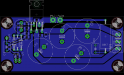
Turn C1 180deg to have the LSP1 at the bottom. Connect from R2 into that pad.
Keep a strait line from C1/11 top pads to the R3 as you had it before.
Then run the gnd from the input to the audio ground around the C1.
Should be easy...
Keep a strait line from C1/11 top pads to the R3 as you had it before.
Then run the gnd from the input to the audio ground around the C1.
Should be easy...
I have concluded that the Amplifier Output Zobel needs a low impedance connection from output devices to the lowest impedance Decoupling Ground.
If I am correct, then the Zobel MUST be at the output pin and tie into the decoupling ground BETWEEN the four decoupling capacitors.
This would require the pin4 pad to be lengthened slightly and an extra hole added for the Zobel resistor to feed between pins 3&5 to the cap tying in to the PCB at the small gap just below the letter C of C3. This would also require the Zobel resistor to cap junction to "float" above C8.
Last edited:
Is there a physical reason how the Zobel network connects? What I try to ask is, is there a reason why the capacitor must be tied to the ground, or can the network be "turned around" and if not, why? This has newer been quite clear to me. The resistor still sees the same voltage and current and so does the capacitor? Inductance does not change. What does?
Of course there is alternatively no reason not to use a R7.5-R10 capacitor for jumping the tracks so that we can easily get to the connection point you just described.
Of course there is alternatively no reason not to use a R7.5-R10 capacitor for jumping the tracks so that we can easily get to the connection point you just described.
- Status
- Not open for further replies.
- Home
- Amplifiers
- Chip Amps
- please review this pcb design