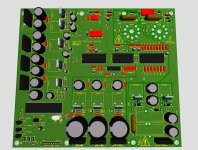
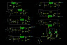


Here are the Section of DIR and DF section...
Asynchronous reclocking, a ripple counter and a digital filter. Interesting times.
Last edited:
+1 rfbrw -- THAT I understood.
Umm .. also, your tubes are missing some DC paths -- no plate load for the 1st stage; no cathode supply for the 2nd.
I do still admire your ambition! 😉
Cheers
Umm .. also, your tubes are missing some DC paths -- no plate load for the 1st stage; no cathode supply for the 2nd.
I do still admire your ambition! 😉
Cheers
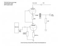
the output wth 6DJ8 Tubes...
You could ground the cathode of the first 6DJ8 stage and bias with the -2mA DC offset from the 1541A through the IV resistor. I would look to Rg <47 ohm. This will lower noise and reduce output impedance at the plate by (~680x33 ohms), open possibility for a single gain stage with output from plate (if the DAC is suitably loaded) and sound much better.
Last edited:
For one better final product, i need the all help possible
Hello, thanks for all sugestions, i have post this project for any welcome helps, but this project are in inicial stage, and i will modify with the all help of the friends for make one more perfect possible final product for make the boards with the more certain of the trusted final product with help of the experts of the forum, (but i not have much experience, only sugestions for try make one good diy product)...
All critical and sugestions are Welcome, but this project are on starting only, and i make some copyes the ideas from the Lite 50 with PCM63 DAC, (design of board power supply, and tube out) and the TDA1541 dac from Analog Metric (with suspect circuit of the reclock), and some circuit ideas from Lampizator sugestions (Lucasz Fikus Lampizator Tutorial 2.0 DIY instruction manual ) and are all certain of one good final product, i will post the new Gerber files from the final and better product, 😉
The initial ideas for start this project
My initial ideas for start this project, are from this products for one base ( i liked and i try apply on this initial project...) And the Genuine TDA1541AS1 (i purchased 3 units. )
My initial ideas for start this project, are from this products for one base ( i liked and i try apply on this initial project...) And the Genuine TDA1541AS1 (i purchased 3 units. )
Attachments
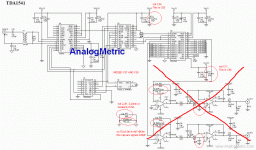
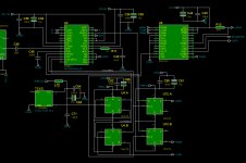
for the non Over sampling, and suspect re-clock too...
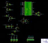
This circuit of reclock, and the SAA7220 are for test only, but i have one strange curiosity for the testing the reclock and the Jitter with one Crystek Oscillator with divided clock from 22.5792Mhz for make 11.2896Mhz for the SAA7220...
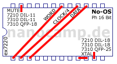
And for final product, i will use thius jumpers for a no-OS DAC:
This circuit of reclock, and the SAA7220 are for test only, but i have one strange curiosity for the testing the reclock and the Jitter with one Crystek Oscillator with divided clock from 22.5792Mhz for make 11.2896Mhz for the SAA7220...
And for final product, i will use thius jumpers for a no-OS DAC:
Attachments
Hope someone with more experience with these parts chimes in -- you'll surely get better advice. But here's what I've noticed:
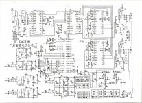
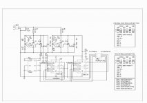
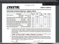
- the CS8412 FILT pin circuit, C40 / R11, should use AGND, the next pin over; avoid DGND
- the FSYNC and SCK pins can be inputs or outputs, but both must be the same; see JPG attached
But that isn't the biggest problem. I think I see what you're trying to accomplish -- providing a local, higher stability clock. But the only way I know of to do that is with a FIFO. Try Search on this forum, there are several projects in various phases of completion, and it is not a trivial undertaking. Without it there is no way to maintain frequency lock, let alone phase lock, with the recovered clock from the incoming RS422 stream. And when the inevitable mis-match happens it doesn't sound good; neither does a succession of Mutes, even if they're brief.
Just my 2 cents ..
Cheers
Attachments
FIFO
Thank you again!! Yes, I will search, thank you for your kindness!!!
My all Best Regards.
Hope someone with more experience with these parts chimes in -- you'll surely get better advice. But here's what I've noticed:
- the CS8412 FILT pin circuit, C40 / R11, should use AGND, the next pin over; avoid DGND
- the FSYNC and SCK pins can be inputs or outputs, but both must be the same; see JPG attached
But that isn't the biggest problem. I think I see what you're trying to accomplish -- providing a local, higher stability clock. But the only way I know of to do that is with a FIFO. Try Search on this forum, there are several projects in various phases of completion, and it is not a trivial undertaking. Without it there is no way to maintain frequency lock, let alone phase lock, with the recovered clock from the incoming RS422 stream. And when the inevitable mis-match happens it doesn't sound good; neither does a succession of Mutes, even if they're brief.
Just my 2 cents ..
Cheers
Thank you again!! Yes, I will search, thank you for your kindness!!!
My all Best Regards.
Last edited:
+1 for Rick Pa Stadel :
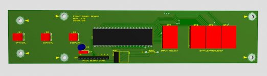
I will hack this board by injecting I2S just before the TDA 1541A with care :short length so some 3d stacking receiver board on the blue pcb.
JLSounds spidf/usb to I2S board
Lorien Wave I/O - spidf/usb to I2S- board
perhaps IanCanada FifoPi with spidf hat : but first check the I2S is ok fr the TDA1541A.
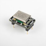
You will save monney, time, many god hours of good listening. All the boards have good enough clocks for the TDA1541A (I own one with Crysteck clocks).
I will hack this board by injecting I2S just before the TDA 1541A with care :short length so some 3d stacking receiver board on the blue pcb.
JLSounds spidf/usb to I2S board
Lorien Wave I/O - spidf/usb to I2S- board
perhaps IanCanada FifoPi with spidf hat : but first check the I2S is ok fr the TDA1541A.
You will save monney, time, many god hours of good listening. All the boards have good enough clocks for the TDA1541A (I own one with Crysteck clocks).
- Home
- Source & Line
- Digital Line Level
- Please Help for SPDIF interface on TDA1541 dac