It's going to take a little while. I just finished the layout of the latest OPS board. The chassis won't be here until 3/10 because of Chinese New Year in China. Still need to set up a test jig to match transistors, test bed to build the amp on a wood board for easy modifying. Just bought two of the 24V switching supply for general testing and maybe for PS for a pure class A design............Hurry up and actually build something... anything...
Use a sense transistor instead of the LED to maximise swing if are going with the active CCS.
It's a long road, this is my first SS amp, have to get a lot of stuffs to set up shop.
Re. the layout:
You should interleave the output transistors to improve cancellation of radiated fields e.g. PNP NPN PNP NPN || PNP NPN PNP NPN not PNP PNP PNP PNP || NPN NPN NPN NPN
You should interleave the output transistors to improve cancellation of radiated fields e.g. PNP NPN PNP NPN || PNP NPN PNP NPN not PNP PNP PNP PNP || NPN NPN NPN NPN
Q20 & Q21 should be high speed, high gain, low Vce small signal transistors, since they pass only the bias voltage. That is one of the great advantages of this topology.
Q1 & Q5 can be any old slow TO-126 that has adequate Vce. You don't need to use these precious CRT drivers here any old BD139/BD140 will suffice.
Your bias generator does not have enough gain for a symmetrical VAS, but I have told you this already.
Your output Re's are too small, but I have told you this already also.
I have been working on this since last night, it's a lot harder. Unlike people that run traces, I use ground and power plane, it's a lot harder to fit in two layers. I managed to do that, but now the challenge is to put the bias transistor on top of one of the power transistor to track the temperature.Re. the layout:
You should interleave the output transistors to improve cancellation of radiated fields e.g. PNP NPN PNP NPN || PNP NPN PNP NPN not PNP PNP PNP PNP || NPN NPN NPN NPN
All NPN on one side and PNP on the other side is a lot easier. My Acurus is like that and has no problem with radiation. Particularly I use power and ground plane with bypass caps right on the collector of the power transistor to the ground plane. That makes a day and night difference.
I'll keep trying the NPN PNP and see whether I can keep everything in and in good layout.
Q20 & Q21 should be high speed, high gain, low Vce small signal transistors, since they pass only the bias voltage. That is one of the great advantages of this topology.
Q1 & Q5 can be any old slow TO-126 that has adequate Vce. You don't need to use these precious CRT drivers here any old BD139/BD140 will suffice.
Your bias generator does not have enough gain for a symmetrical VAS, but I have told you this already.
Your output Re's are too small, but I have told you this already also.
I am using 3EF, the load on the bias generator is very light. You think it's necessary? I remove the CFP circuit because I don't want to deal with stability issue if I don't have to.
I have to look at the pin out and also thermal couple of the TO-92 transistors. I am designing so I have the TO-126 pre-driver screwed right onto the bigger driver transistor to track temperature. So the physical mating surface is much more important to me than the little beta and fT gain using a small transistor. With 3EF, I think it is a lot more forgiving on this.
From the simulation, these transistor is not the most important thing. I found the Oliver's optimization and using TMC makes the most difference. I lower the Re of the big transistor from 0.22 to 0.12 because it makes a difference in the distortion. Not that I trust D Self that much, but he is strong advocate for 0.1ohm. I think this affect only the quiescent bias current, when there is large signal, there will be so much current through the resistor that there will be a lot of voltage drop across even th 0.1ohm resistor.
Last edited:
Think of this possibility.
You forget to hook the IPS outputs to the OPS 😱. I actually did this.
My two MJE340 Vbe's survived , the rail fuses blew and the amp lived to
function another day.
Using a 5V zener across the Vbe (whole circuit)could be another option , but the possibility
of reverse leakage or other "badness" is magnified by the high Z EF3.
The Mje340 seems to have exactly the reverse thermal co-efficient of
my NJW0302/0281's. My bias is < (point).2-3mv from 10C -50C.
So , things are right here !
I never tried the BD's , I have used 2sc3503's , they give the whole OPS
a slight negative co-efficient.
The japanese OEM's use a select 2sb/sd to-92 as Vbe , most likely matched to
their Sanken output devices. Just an observation. 🙂
OS
Your bias generator does not have enough gain for a symmetrical VAS, but I have told you this already.
You are right, I simulated 20KHz 1.5Vin(30V output). The 3H is almost 8dB lower to slightly under -70dB. That is 98dB below the fundamental peak. This is 20KHz and high power.
My problem is how am I going to fit that in. It is very hard to do it as is already as I have to put the bias transistor on top of the big transistor to get thermal tracking. If I can do it, it will be good. I have the PNP predriver screw onto the NPN driver, the NPN pre-driver screw onto the PNP driver. AND I have the bias transistor screw onto one of the big power transistor. This is the best thermal coupling it can be bar none.
I am simulating 1KHz 1.5Vin 30V output. I'll update later as it takes about 2 hours to do one simulation. Keep the comments coming, it might take a while to get back to you, but I am reading.
Thanks
Attachments
Last edited:
I have to retract the last post. I spent the whole day running 1KHz at 1.5Vin and 0.35Vin. I ran 20KHz 0.35Vin. There is absolutely no difference between the CFP bias multiplier vs the simple one transistor bias multiplier. I started questioning what's going on. I redo the 20KHz 1.5Vin like the last post, I cannot get back the good result anymore. So I don't know what to think anymore. Basically there is NO difference between the two far as I can tell.
I'll investigate more tomorrow.
I'll investigate more tomorrow.
Nice OPS variant!
Don't think it is necessary to wait a day for usable FFT results. Have a look at the modified example. Does run only a few seconds to get good results.
More LTSpice examples can be found in the thread http://www.diyaudio.com/forums/soli...ormance-class-ab-power-amp-200w8r-400w4r.html
BR, Toni
Don't think it is necessary to wait a day for usable FFT results. Have a look at the modified example. Does run only a few seconds to get good results.
More LTSpice examples can be found in the thread http://www.diyaudio.com/forums/soli...ormance-class-ab-power-amp-200w8r-400w4r.html
BR, Toni
Attachments
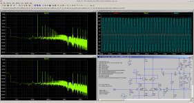
Thanks, I have to learn this. What is the key thing you do to speed it up?Nice OPS variant!
Don't think it is necessary to wait a day for usable FFT results. Have a look at the modified example. Does run only a few seconds to get good results.
More LTSpice examples can be found in the thread http://www.diyaudio.com/forums/soli...ormance-class-ab-power-amp-200w8r-400w4r.html
BR, Toni
Thanks
Think of this possibility.
You forget to hook the IPS outputs to the OPS 😱. I actually did this.
My two MJE340 Vbe's survived , the rail fuses blew and the amp lived to
function another day.
Using a 5V zener across the Vbe (whole circuit)could be another option , but the possibility
of reverse leakage or other "badness" is magnified by the high Z EF3.
The Mje340 seems to have exactly the reverse thermal co-efficient of
my NJW0302/0281's. My bias is < (point).2-3mv from 10C -50C.
So , things are right here !
I never tried the BD's , I have used 2sc3503's , they give the whole OPS
a slight negative co-efficient.
The japanese OEM's use a select 2sb/sd to-92 as Vbe , most likely matched to
their Sanken output devices. Just an observation. 🙂
OS
Do you mean bad things can happen if I forgot to connect the +IN and -IN from IPS/VAS? How about putting a1M resistor from the base of Q9( bias transistor) to ground. So even if it's open, it will pull the junction close to ground.
Here is the schematic of the latest version. I layout so I can screwed the pre-drivers and the drivers together so the NPN and PNP track the temperature quickly and closely. I also layout to screw the bias transistor Q9 to one of the power transistor Q17 so the bias transistor track the temperature of the power transistor.
I think this is as good as using the NJL type of transistor. Now the OPS achieves completely thermal tracking.
I don't know what transistor have the same tempco, If you have better suggestion of the TO-126 pre drivers that can track the power transistor and the driver transistor I use, let me know. But I really prefer it's in TO-126 as I want to screw onto the big transistors. I don't want TO-92.
Thanks
Attachments
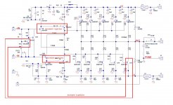
Here is the pcb layout for NPN PNP NPN PNP NPN alternate power transistor at the output stage. All collector of the power transistors and drivers have 0.1uF and 10uF bypass almost point to point from the collector pin of the transistor straight to ground plane. The speaker output and the output return are close to the middle of the power transistors so I literally have half the transistor on each side so the current between the two halves are close. I managed to have a ground plane, power planes for the rail voltages and filtered rail voltages for the pre-drivers.
I also designed so the predrivers are screwed onto the big driver transistors to have close temperature tracking.
I have to bias transistor ( Q9) screw onto one of the power transistor (Q17) to get good temperature tracking. The OPS has temperature tracking for all three stages of the emitter followers.
It's a lot of work to layout this, but I don't have to compromise anything. I have to create parts of different length to fit the tight layout.
Attachments
Last edited:
IMHO: don't think that the interleaving of OPS transistors is a good choice or does give better distortion results. The currents can not cancel out each other as they always represent the opposite half wave of the output signal. Is there a document out there which describes this bjt interleaving in depth?
BR, Toni
BR, Toni
Thanks, I have to learn this. What is the key thing you do to speed it up?
Thanks
IMHO we do not need millions of data points for a single sinus wave to get useful FFT results. You can experiment with the "fft" parameter to increase or decrease the simulation step size and compare the results.
BR, Toni
interleaving of high current devices is probably a good idea.IMHO: don't think that the interleaving of OPS transistors is a good choice or does give better distortion results. The currents can not cancel out each other as they always represent the opposite half wave of the output signal. Is there a document out there which describes this bjt interleaving in depth?
BR, Toni
I think R.Cordell mentions it.
It allows for much smaller LOOP AREAS in the traces passing impulsive currents. That is always a good thing in minimising interference.
It also helps with thermal balance between the upper and lower halves of a push pull output stage.
If the layout is perfect, even if you put all PNP on one side and all NPN on the other side, it dose not hurt that much. Loop current that cause radiation can form if current has to go through a bigger loop. When I first layout the board, I had all NPN on one side and PNP on the other side. But I use ground and power plane with 0.1u and 10uF from the collector to the ground plane on every power transistor. Loop area is very small, as all current are going to the ground on the spot. That's why it's so important to have bypass cap and use power and ground planes to minimize loop and path inductance.
But after Christian ( Ranchu 32) mentioned again, I redo the layout and managed to do NPN PNP NPN PNP.............. So I am happy. It's not easy, to get wide uninterrupted planes, I had to create resistors of different spacing on the fly to ensure the plane is uninterrupted. Had to turn some components in funny angle to optimize the layout. I had to modify the schematic according to the layout.
Let me put it in another way, I will pick the layout with NPN on one side and PNP on the other side any day if there is ground and power plane with bypass caps for every transistor OVER alternate transistors without planes and without bypass caps. It's all about the layout, that's where the battle won or lost.
Last edited:
Can you post the latest version of your layout please. Do you intend to provide PDF and/or Gerbers for those that wish to build your output board?
Have you thought about how you will interface your input and output board?
Have you thought about how you will interface your input and output board?
I posted in post #92.Can you post the latest version of your layout please. Do you intend to provide PDF and/or Gerbers for those that wish to build your output board?
Have you thought about how you will interface your input and output board?
Last edited:
those who would like to learn more about power amplifier designs, this is a good source from Motorola.....http://www.diyparadiso.com/datasheets/anpoweramp.pdf
Interesting layout Alan, I quite like it. I gather the power output are designed to be parallel and underneath the PC board? There is a little wasted space here. You might consider repositioning some components so that the output transistor pads run along the edge, so that the output transistors can be mounted perpendicular to the PC board.
Do you worry about those long thin traces providing drive the the outputs? You could reposition the driver circuitry to the middle of the PC board perhaps and make the board a little shorter. The board area removed from the lower side could be added to the upper side.
- You might want to space the outputs for better thermals.
- You'll definitely need to heatsink the main drivers.
- Status
- Not open for further replies.
- Home
- Amplifiers
- Solid State
- Please comment on my OPS design