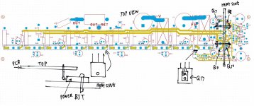
Here is the more detail description how I mount the board and where theseparate heatsink for the drivers (Q7 & Q11) and pre-drivers (Q8 & Q10) are mounted together so they achieve thermal tracking. Also shows how the bias transistor ( Q9) is mounted on top of the power transistor Q17 so the bias multiplier achieve thermal track with the big power transistor.Interesting layout Alan, I quite like it. I gather the power output are designed to be parallel and underneath the PC board? There is a little wasted space here. You might consider repositioning some components so that the output transistor pads run along the edge, so that the output transistors can be mounted perpendicular to the PC board.
Do you worry about those long thin traces providing drive the the outputs? You could reposition the driver circuitry to the middle of the PC board perhaps and make the board a little shorter. The board area removed from the lower side could be added to the upper side.
- You might want to space the outputs for better thermals.
- You'll definitely need to heatsink the main drivers.
The power transistors are mounted from the bottom of the board and bent 90 deg to mount onto the big heat sink. The board is parallel with the main heat sink.
The trace that drive the bases of the big transistors are 60mil (2.36mm) wide. You don't think it's wide enough? I can increase to 75mil ( about 3mm) no problem. But 60mil is quite wide already.
Putting the driver in the middle is impossible. Everything will be bundle up in the middle. Too many planes in the middle and result in thinning the ground and power planes.
If you look at my layout, I have all the high current devices on the left side, then I have the output and power pick-off point all close to the middle of the high current devices. There is no high current around the drivers and pre-drivers. I have the power of the pre-drivers separated by RC network to filter out the ripple on the right side. I tried very hard to keep the traces very short as shown. The only long traces are the base drive for the big transistors and the +IN & -IN. The rest are close to point to point.
Attachments
Last edited:
Thanks Alan, note your driver transistors appear to be oriented the wrong way (the plastic body is facing the heatsink).
60 thou is plenty wide enough.
60 thou is plenty wide enough.
Thanks Alan, note your driver transistors appear to be oriented the wrong way (the plastic body is facing the heatsink).
60 thou is plenty wide enough.
You are scaring me!!!😱
The symbol of the drivers Q7 and Q11 is wrong!!! I checked, the metal part of both the drivers and the pre-drivers (Q8 and Q10) are facing each other and mounted directly onto the heat sink( eg. the metal bottom of Q7 is facing the metal bottom of Q8. The heatsink is sandwiched in between). Please verify for me, I looked at it a few times and it is correct for me. But I don't rule out my eyes doing a trick on me.
All the BJT are standard pin out where #1 is base, #2 in the middle is collector and #3 is emitter.
Thanks
Last edited:
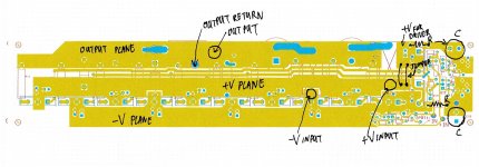
This is the power plane showing the power feed, output and output return. The output and output return to the ground plane is almost in the middle of the power transistors so the current is symmetrical.
+V for Q7 has to be jumpered from the main +V plane in order to let the base drive traces to go through.
Two RC network filtering the rail voltage before feeding the pre-drivers Q8 and Q10.
The two 1000uF cap is in between the power transistors on the left side and the drivers on the right side. Any ripple current is filtered by the big caps before feeding the drivers.
I am happy with the layout. After 2 tries, this is the best. I just want to sit on it for a few days, wait for the parts to arrive, measure the parts to verify the dimensions and sent to board out for fab.
Attachments
Last edited:
Compare CFP bias circuit with single transistor bias circuit.
I spent over a day comparing OPS distortion between CFP bias circuit vs simple single NPN bias multiplier using LTSpice VI. I spent the time to run with fine time steps to get more accurate and good looking FFT graph. Attached are the FFT for 1KHz and 20KHz at 7Vpeak and 30Vpeak output.
There is NO discernible difference between the two. I even ran comparison at 5KHz, there is no difference. I don't believe it is necessary using CFP circuit here. I think it's mainly because this is a 3EF, loading of the VAS is very very light. The current of the VAS is 10mA which is even higher than the idle current of the first pre-driver stage.
It might be a different story if it's 2EF output stage. But not in this case at all.
Attachments
-
3EF diamond amp 200mA alone.asc27 KB · Views: 70
-
3EF diamond 5stages 20KHz 1.5Vin 5mS 0.0005uS 200mA Olivers 20 2.2 0.13ohm TMC single bias.pdf82.6 KB · Views: 73
-
3EF diamond 5stages 20KHz 1.5Vin 5mS 0.0005uS 200mA Olivers 20 2.2 0.13ohm TMC.pdf80.3 KB · Views: 81
-
3EF diamond 5stages 20KHz 0.35Vin 5mS 0.0005uS 200mA Olivers 20 2.2 0.13ohm TMC single bias.pdf62.7 KB · Views: 68
-
3EF diamond 5stages 20KHz 0.35Vin 5mS 0.0005uS 200mA Olivers 20 2.2 0.13ohm TMC.pdf77.5 KB · Views: 58
-
3EF diamond 5stages 1KHz 1.5Vin 50mS 0.005uS 200mA Olivers 20 2.2 0.13ohm TMC single bias.pdf115.2 KB · Views: 85
-
3EF diamond 5stages 1KHz 1.5Vin 50mS 0.005uS 200mA Olivers 20 2.2 0.13ohm TMC.pdf113.4 KB · Views: 77
-
3EF diamond 5stages 1KHz 0.35Vin 50mS 0.005uS 200mA 20 2.2 0.13ohm TMC single bias.pdf87.3 KB · Views: 78
-
3EF diamond 5stages 1KHz 0.35Vin 50mS 0.005uS 200mA Olivers 20 2.2 0.13ohm TMC.pdf89.4 KB · Views: 77
Interesting. I gather the first input stage you build will be a fully balanced design. That being the case I will be interested to follow your progress.
You are scaring me!!!😱
All the BJT are standard pin out where #1 is base, #2 in the middle is collector and #3 is emitter.
TO126 parts have a reverse pinout with respect to TO220
You are right, all the TO-264, TO-247 and TO-220 are the same with base =1 collector =2 and emitter =3. But the two TO-126 I use is opposite.TO126 parts have a reverse pinout with respect to TO220
I have to switch the bias transistor Q9, Q7 and Q11 is fine. They don't generate heat. Being screw on top of the driver transistors to track the temperature is going to be much better than if they all just screwed onto the heat sink side by side, even if it's the plastic part that is in contact.
Thanks
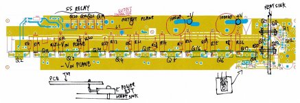
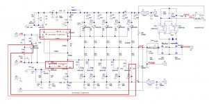
I just finish the pcb. I added the SS relay for speaker connection. The detection circuit is going to be off board as I really run out of room. It is standard SS relay design except I parallel two MOSFETs to reduce the ON resistance by half. I am using MOSFET with only 3.6mohm RDSON. With 4 transistor, the on resistance is going to be only 3.6mohm. Attached is the final schematic and the layout.
This is pretty much it. It is getting very tight as it really cut into the planes and is hard to keep a wide uninterrupted plane now.
Please let me know what you think.
Thanks
This is pretty much it. It is getting very tight as it really cut into the planes and is hard to keep a wide uninterrupted plane now.
Please let me know what you think.
Thanks
Attachments
-
 3EF Diamond double SS relay long ground and trace.jpg553.1 KB · Views: 162
 -
 3EF Diamond double SS relay long power and trace.jpg314.8 KB · Views: 181
 -
3EF diamond power plane and traces.pdf175 KB · Views: 76
-
3EF diamond ground plane.pdf156.5 KB · Views: 77
-
3EF diamond trace and components.pdf55.1 KB · Views: 66
-
 3EF diamond doube SS relay.jpg219 KB · Views: 189
Last edited:
I just received the KSC3503, it's plastic on both side. Mounting wise, I don't think it matters the top or the bottom side screwed onto the heatsink.TO126 parts have a reverse pinout with respect to TO220
The problem I need to verify is how can I tell which side is the top!!! According to the data sheet, the top side has 3 indented circles, two above the hole and one below. That's the only thing I can see.......of cause the side with 3 circular indent also has the part number and marking. Can I assume that's the top side?
I just received the KSC3503, it's plastic on both side. Mounting wise, I don't think it matters the top or the bottom side screwed onto the heatsink.
The problem I need to verify is how can I tell which side is the top!!! According to the data sheet, the top side has 3 indented circles, two above the hole and one below. That's the only thing I can see.......of cause the side with 3 circular indent also has the part number and marking. Can I assume that's the top side?
Yes, the one with the markings is the top side. The bottom side is just flat.
Thanks, I am almost ready to sent the board out.
I layout so Q7 is screwed together with Q8, Q10 screwed to Q11. Since the KSC and KSA package are plastic on both sides, I am debating whether I should screw the top to the heat sink or the bottom. The layout is a lot better if I screw the top side to the heat sink.
If you look at the transistor side way, the distance from the bottom to the plane of the pins is almost double the distance from the pins to the top. If the transistor inside is on the plane of the pins, it is actually closer to the top. These two KSC and KSA do not have to dissipate any power, it is only for sensing the temperature of the big driver transistors.
I am hoping to send the board out tomorrow. I received more of the parts already. Time for the rubber meets the road!!!!😱
In most cases I screw the Vbe multiplier sensor with the bottom side to the heatsink, but in one of the recent designs, due to the layout mistake, I had to screw it up side down. No difference. Same tempco, bias tracking, etc.
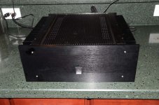
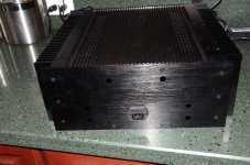
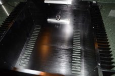
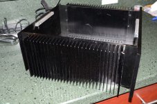
Just received my amp chassis. Attached is the pictures. It's a beautiful chassis, better looking than my Acurus. The heat sink fins are 1 3/4" long, the fins are 5 3/4" wide and the heat sink is 11" long total. It said it's for 300W, I believe it.
I received the 625VA 30V-30V toroidal PT and transistors and parts are trickling in. The rubber is going to hit the road soon.
I just sent out the OPS board for fab, it'll be back by the middle of the month. I am finishing up the IPS/VAS board to be sent out.
I received the 625VA 30V-30V toroidal PT and transistors and parts are trickling in. The rubber is going to hit the road soon.
I just sent out the OPS board for fab, it'll be back by the middle of the month. I am finishing up the IPS/VAS board to be sent out.
Attachments
Last edited:
My exact chassis. Looks like it too had a rough ride from hong kong.
PS - think twice , drill once.
OS
PS - think twice , drill once.
OS
Yeh, it's the prettiest chassis on ebay I can find with big heatsink. I even bargain with the guy to get down to $270USD total. He is tricky, he sell the chassis for $125 but $145 for shipping. But I figure I am not going to return it. I already put everything together to verify everything fit. There is no scratch on the surface at all, just a lot of dust from the packing material. It looks dusty only under the camera flash.My exact chassis. Looks like it too had a rough ride from hong kong.
PS - think twice , drill once.
OS
The heat sink is so big and thick, that's the reason I was not worry about running 200mA per stage with 5 stages total.
I ordered a pair of different heatsink. I am planning to put everything on a wood board, test and work on it before I even put into the chassis. So any drilling mistake will be on the spare heatsink.
I even bought and received a pair of 24V 15A switching supplies. I am going to try with that and jack up the current to 300mA per stage to really run in Class A. I am not ruling out putting the 24V switchers into the chassis if that sounds better.
Last edited:
Yeh, it's the prettiest chassis on ebay I can find with big heatsink. I even bargain with the guy to get down to $270USD total. He is tricky, he sell the chassis for $125 but $145 for shipping. But I figure I am not going to return it. I already put everything together to verify everything fit. There is no scratch on the surface at all, just a lot of dust from the packing material. It looks dusty only under the camera flash.
The heat sink is so big and thick, that's the reason I was not worry about running 200mA per stage with 5 stages total.
I ordered a pair of different heatsink. I am planning to put everything on a wood board, test and work on it before I even put into the chassis. So any drilling mistake will be on the spare heatsink.
I even bought and received a pair of 24V 15A switching supplies. I am going to try with that and jack up the current to 300mA per stage to really run in Class A. I am not ruling out putting the 24V switchers into the chassis if that sounds better.
You will have no issues to run your OP's a little hot. I run mine all day at house-shaking levels (under 40C),
You are still on that "class A" kick ?? AB's run and sound better 60-100ma -
period ! They DO NOT sound better "hot" (high bias) 😕😕.
Oh , well ... you will learn 🙄 .
OS
Why AB and 100mA sounds better. The best result is when there is no cross over distortion. I think the most important for me is Class A for the first 10W. I am actually very interested in the Haraga 20W Class A. I might try that also on the wood board before deciding which one to put into the chassis.
Yes, I have my Acurus raise to 100mA per stage and it does sounds better than the original cold bias. I still want to try 200mA.
Come to think about it, I did raise the Acurus to 200mA and it did not improve as much as I thought, but it's not worst than at 100mA. But the Acurus gets too hot as it has 80V rail instead of 40V like my new design. Also, I still have 0.5ohm emitter resistor in the Acurus, I should parallel up another 0.5ohm to get Oliver's optimization.
BTW, I bought 35 of each MJL3281 and MJL1302 so I can find matching 5 for each channel. I bought 100 of each of the BC556 and BC546 so I can pick the matching differential pair for the IPS.
Alan, have you investigated Self's Class XD scheme detailed in APAD6? Seems like a more efficient and effective way to get a nice fat "Class A" region if that's your thing, without resort to lots and lots of output transistors.
No, is it in the book? I have to find the book!!! I am very disgusted with the book and have not even touch it. Don't like it at all.Alan, have you investigated Self's Class XD scheme detailed in APAD6? Seems like a more efficient and effective way to get a nice fat "Class A" region if that's your thing, without resort to lots and lots of output transistors.
- Status
- Not open for further replies.
- Home
- Amplifiers
- Solid State
- Please comment on my OPS design