This is a fairly unique kit, and there is enough information here to freely build your own, modify another off the shelf DAC etc. I have received mine a couple of weeks ago, but been far too busy to assemble it at the moment
I can say for the amount of components you get, as well as the time saved trying to modify something or develop something on your own, this represents fantastic value - i can't wait to build mine!
I can say for the amount of components you get, as well as the time saved trying to modify something or develop something on your own, this represents fantastic value - i can't wait to build mine!
I am glad that everyone is standing up to the spirit of DIY. We are all proud of our projects because each one is uniquely created.
We also share openly with the community whenever we find a better way to do it so that everyone benefits from it.
If you buy a commercial gear, it is your choice. You just lose the chance to be part of this family.
Nelson Pass once said "Audio DIYers are the happiest people".
We also share openly with the community whenever we find a better way to do it so that everyone benefits from it.
If you buy a commercial gear, it is your choice. You just lose the chance to be part of this family.
Nelson Pass once said "Audio DIYers are the happiest people".

Posts by a sock puppet have been removed. If any of you were caught up in that and quoted/commented on any of those posts then they will have gone as well 🙂
Finally up and running! Thank you @abraxalito for all help you provide to me.
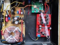
New power supply and PhiDAC in old DIY 1543 DAC case I had.
First impressions are great, I think PhiDAC is dac you can listen all day and have a smile on your face.
New power supply and PhiDAC in old DIY 1543 DAC case I had.
First impressions are great, I think PhiDAC is dac you can listen all day and have a smile on your face.
Attachments
Last edited:
Yes that is correct with the small change that U9 is now TL431 (CJ431 shown on the schematic). We made that change for greater robustness in the unlikely case of a failed DAC chip.
For populating the board its probably easiest to work from the graphic linked to in the first post on this thread.
For populating the board its probably easiest to work from the graphic linked to in the first post on this thread.
Last edited:
Finally up and running! Thank you @abraxalito for all help you provide to me.
New power supply and PhiDAC in old DIY 1543 DAC case I had.
First impressions are great, I think PhiDAC is dac you can listen all day and have a smile on your face.
You optimised on short output cables... maybe it would have been better to turn the boards so that the digital interconnect was shorter and still just a bit longer output cables - which should probably be twisted.
//
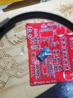
The LEDs (D3-D1) are oriented alternately. D3 and D1 have cathodes (green dot on top) towards R17 so looks like you need to reverse the orientation you're showing in the picture for D3. D2 has cathode towards Q8.
My parts kit supplied includes 2 CJ431 and one packet labelled as TL431. The marking in the part labelled as TL431 is 4B 8A.
Is the part 4B 8A TL431?
I read that CJ 431 has been changed to TL431 for greater stability. Is this true?
Is the part 4B 8A TL431?
I read that CJ 431 has been changed to TL431 for greater stability. Is this true?
As regards the TL431 yes 4B indicates a TI-sourced TL431AIPK (SOT-89). See post #47 above in respect of the substitution of CJ431.
On 74HC86D and other SOIC parts, these packages have a chamfer on the side of pin1 so your picture does indeed show the correct orientation.
On 74HC86D and other SOIC parts, these packages have a chamfer on the side of pin1 so your picture does indeed show the correct orientation.
Quoted from another post
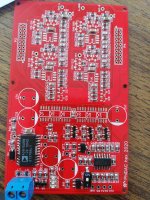
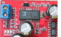
Apply 12V from a supply limited to ~150mA short circuit current to the power input pins at top left. If all is fine the three red LEDs will illuminate and you can check TP1 (5.5V), TP2 (8.3V) , TP3 (10V), TP4 (4.6V) and TP5 (2.5V). These voltages are all measured relative to the 0V power input terminal. Also measure across R56,R65 & R70 (these are level shifting resistors) - the reading across each should be ~4.6V.
Assuming all those are correct within ~0.1V you can progress to 'step 2'.
I have populated up to here. Plan to put a 12 v input to check the test points on board. In the current state of my partially populated board, will the measurements of voltage at TP 1 to TP4 valid?
Although you've populated all the passives on the right side of the board I believe all the TP voltages (including TP5) will be unaffected by that.
All voltages at TP 1 to 5 measure within 0.1 to 0.15v.
Proceed to stage 2.
Quote
At 'step 2' solder the DAC chips (after powering down, of course!). To be extra-cautious you can replace L9 (a ferrite bead, FB) with a 1R resistor. This will allow you to check the DAC supply current - as they're recycled parts there's the very slim chance you may get one which draws too much current. On powering up again double check the voltage across the three level shift resistors again (4.6V) and also across C57. The latter should be ~3.6V. The supply current should be about 22mA, corresponding to 22mV measured across the 1R test resistor.
Unquote.
What are the 3 level shift resistors? Is it refer to voltage at TP4?
Level shift resistors are R56,R65 and R70 on the schematic. They raise the levels at the output of the HC86 to be compatible with the DACs' logic levels. Since the DACs sit atop the TL431 (U9) their logic '0' is 4.6V and logic '1' is above 6.6V.
Incidentally the 22mA figure was estimated from the datasheet rather than measured in-circuit. Turns out in the circuit the current drawn is less when the outputs aren't connected (as here - the filter's not yet installed) so ~17mA is more like the current to expect.
Incidentally the 22mA figure was estimated from the datasheet rather than measured in-circuit. Turns out in the circuit the current drawn is less when the outputs aren't connected (as here - the filter's not yet installed) so ~17mA is more like the current to expect.
Last edited:
- Home
- Vendor's Bazaar
- PhiDAC hex kits with pre-built filters