For one, they define hotspots for components with rectangles, when there are so many items within close proximity to each other you end up moving more or wrong components, which moved traces you may not of noticed. This would of been avoided, if they defined the hotspot as an outline of the component. I don't see options for layered components, like transistors on horizontal heat sinks, double mounting holes are flagged as an error. I do like dip trace a lot, but sometimes $%%@$.
MI
I found it frustrating when I was first starting to use it, but have it figured out now. I used Sprint for a short time before switching to DipTrace. I was saving my files on Dropbox at that time. I would close a design, then finish it from another computer at a later time. When I would restart the first computer at a later time, it would overwrite parts of my finished files. I had a few junk boards made before I figured that out. Diptrace is smart enough to not let me alter a file that isn't finished saving from another computer.
I use Botech Circuits in China and have always had excellent pcb's and 2 weeks from order to pcb's at my door.
Min order is 5 for small pcb's but there price is about 1/3 of what I pay in the UK.
botechcircuits@gmail.com
Min order is 5 for small pcb's but there price is about 1/3 of what I pay in the UK.
botechcircuits@gmail.com
Hey, you guys wanna to give this Company Shenzhen SYS technology( site www.syspcb.com ) a try? PCB maker in China since 2006.
Our first order from PCBWay gave pretty good boards in a fast turn-around-time. (4days, Friday->Wednesday)
The board is 100*160mm 6/6mil tracks and 12/24mil vias. Came out nice, registration is good (still not perfect), mask opening could be a bit smaler to my needs.
But have a look at the pictures.
The board is 100*160mm 6/6mil tracks and 12/24mil vias. Came out nice, registration is good (still not perfect), mask opening could be a bit smaler to my needs.
But have a look at the pictures.
Attachments


Last edited:
Good experiences so far with pcbway!
I was going to start a thread about these folks after having a few good ordering experiences, but I just found this one via search.
Disclaimer: I'm not affiliated with pcbway in any way, just a happy customer at the moment. 🙂
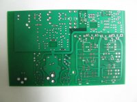
I first found the company a few months ago via pcbshopper.com, a board comparison service that Mark Johnson had linked to in another thread. I've been using Seeed Studio in China for the last couple of years with good results, but the prices have been creeping up, especially with the shipping. The pcbway price couldn't be beat, the processing time was incredible (short!) and they ship via DHL express for just $25 (I've been paying $35-$45 at Seeed Studio). Since then I've run the 3 boards in the photos below. I'm using Eagle V7 pro for the layout.
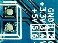
The first board is just a top-slot carrier board for another PC board, so (almost) no circuitry. Pcbway processed the big milled-out hole in the center correctly. The hole is to allow heat from parts on a board below to make it up to the top of the case and out some rear panel vents. Lol, I figured this was a good first test board. If they screwed up a board with one trace on it, that would have been the end. 😀
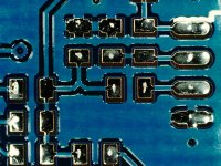
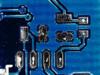
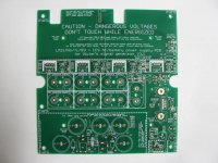
The next board was a lot more involved with 4 layers. Pcbway got it right! I've built up a couple of the boards now and they work perfectly. The finish on the board is just HASL. This design has parts on both sides of the board. It would have had text on the bottom for all the SMD parts if I didn't screw up one library part on my end and put the text on the top by mistake.
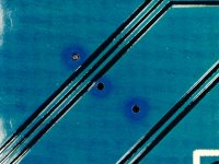
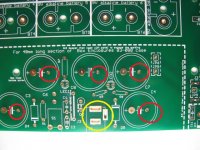
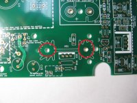
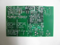
The third board (a 2 layer but large - 148mm by 143mm) is the most interesting because they did make a fabrication mistake, as the last two photos show (the red circles). The pads for the large heatsink were missing (one through-hole plated but the other didn't) and half the large electrolytic pads mysteriously shrunk. The yellow circle isn't a mistake, those are through-hole plated slots that pcbway processed perfectly! Mistakes can always happen, especially with the super-short timeframe these folks build the board in. The true test is how a company deals with it when a problem comes up.
Well I'm happy to say these folks passed the test. Their customer service got right back to me via email and had an in-house engineer look into it. The result was an error in a manufacturing file on their end, so they re-did the board at their expense. I also learned that all pads have to have a circuit attached, or they won't through-hole plate (what happened to the lower heat sink mount), something to keep in mind with this processor. This board was ENIG (gold) and the re-do was still in gold, even though I told them HASL would be OK (I was just curious how their ENIG finish looked). Even better they were willing to use an updated set of Gerbers for the re-do, since I had made a few updates since the original. I was pretty happy about that and volunteered to cover the $25 for the DHL express shipping again, although I presume they would have paid that too.
I'm certainly happy enough with the results to keep sending boards in! I'm getting another one together right now in fact.
I was going to start a thread about these folks after having a few good ordering experiences, but I just found this one via search.
Disclaimer: I'm not affiliated with pcbway in any way, just a happy customer at the moment. 🙂
I first found the company a few months ago via pcbshopper.com, a board comparison service that Mark Johnson had linked to in another thread. I've been using Seeed Studio in China for the last couple of years with good results, but the prices have been creeping up, especially with the shipping. The pcbway price couldn't be beat, the processing time was incredible (short!) and they ship via DHL express for just $25 (I've been paying $35-$45 at Seeed Studio). Since then I've run the 3 boards in the photos below. I'm using Eagle V7 pro for the layout.
The first board is just a top-slot carrier board for another PC board, so (almost) no circuitry. Pcbway processed the big milled-out hole in the center correctly. The hole is to allow heat from parts on a board below to make it up to the top of the case and out some rear panel vents. Lol, I figured this was a good first test board. If they screwed up a board with one trace on it, that would have been the end. 😀
The next board was a lot more involved with 4 layers. Pcbway got it right! I've built up a couple of the boards now and they work perfectly. The finish on the board is just HASL. This design has parts on both sides of the board. It would have had text on the bottom for all the SMD parts if I didn't screw up one library part on my end and put the text on the top by mistake.
The third board (a 2 layer but large - 148mm by 143mm) is the most interesting because they did make a fabrication mistake, as the last two photos show (the red circles). The pads for the large heatsink were missing (one through-hole plated but the other didn't) and half the large electrolytic pads mysteriously shrunk. The yellow circle isn't a mistake, those are through-hole plated slots that pcbway processed perfectly! Mistakes can always happen, especially with the super-short timeframe these folks build the board in. The true test is how a company deals with it when a problem comes up.
Well I'm happy to say these folks passed the test. Their customer service got right back to me via email and had an in-house engineer look into it. The result was an error in a manufacturing file on their end, so they re-did the board at their expense. I also learned that all pads have to have a circuit attached, or they won't through-hole plate (what happened to the lower heat sink mount), something to keep in mind with this processor. This board was ENIG (gold) and the re-do was still in gold, even though I told them HASL would be OK (I was just curious how their ENIG finish looked). Even better they were willing to use an updated set of Gerbers for the re-do, since I had made a few updates since the original. I was pretty happy about that and volunteered to cover the $25 for the DHL express shipping again, although I presume they would have paid that too.
I'm certainly happy enough with the results to keep sending boards in! I'm getting another one together right now in fact.
Attachments

Last edited:
Normally they accept an additional NPTH drill file (so having 2 drill files, one for plated, another for non-plated holes).
Normally they accept an additional NPTH drill file (so having 2 drill files, one for plated, another for non-plated holes).
I've had this without issues; some of my mounting holes weren't plated and were in a different gerber drill file and came back as expected 🙂
Hey good to know! Having a pad without a circuit attached, like those heatsink mounts, is a pretty common thing that comes up.
Yes, but there shouldn't be any issues if the drill files are right. Problems occur if you just have one drill-file with plated/non-plated holes mixed together. Only then, holes without copper connection or pad are supposed to be non-plated. (I always use 2 files and send manufacturing instructions with)
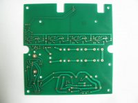
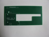
Mine is most likely mixed. I had the earlier V2.0 incarnation of the board processed at Seeed Studio, photo below, and it didn't have the problem with the missing heatsink pads, even without a circuit attached to the lower one.
Attachments
Last edited:
Yeah, depends on the fab house. (My guess, the more hobbyist fabs like seed, elecrow, itead etc. will look closer for "design-flaws"/mixed-up stuff [or have ded. personal])
Better go for the two-files-solution. 🙂
Better go for the two-files-solution. 🙂
If there is a pad drawn on both sides of the board for a heat sink, it should be there and through hole plated. I've never had one dropped because there wasn't a trace connected to it. They've done 40+ sets of boards for me in the past year.
I've never sent more than one drill file. They figure out if through hole plating is required if pads are present. Giving extra instructions gives more opportunity for error. Sending written instructions in English is begging for problems.
I've never sent more than one drill file. They figure out if through hole plating is required if pads are present. Giving extra instructions gives more opportunity for error. Sending written instructions in English is begging for problems.
If there's room for interpretation, instructions clarify things.
If your instructions resulted in errors, the instructions weren't clear. 😉
Confusion about to plate or not in a combined drill file is related to the gEDA and the way, the Herbert's are generated. YMMV.
If your instructions resulted in errors, the instructions weren't clear. 😉
Confusion about to plate or not in a combined drill file is related to the gEDA and the way, the Herbert's are generated. YMMV.
Translating instructions from English to Chinese will never be clear. There's not much room for interpretation from proper Gerber files. Copper is there or it is not. Solder mask is there or it is not. Silkscreen ink is there or it is not. There is a hole at this x y location. Pretty self explanatory. That's why they are the industry standard. Any special instruction neede is on the order page on the website, like quantity, colour,ect.
Seems like it didn't worked out right here, as seen some posts before.
But yes Sir, as you say Sir, you're right Sir! ..

Will you show some of your work please? Cool.
But yes Sir, as you say Sir, you're right Sir! ..
Will you show some of your work please? Cool.
Last edited:
I'm sorry if I offended you with common sense. Look back at most of the complaints through this thread and you'll find most of them were errors in the board files. Do you think it's necessary to write separate instructions to have double sided pads under a heat sink, when the gerbers state this?
No, this should be clear but there is a rare chance where the gEDA puts out Gerber in a "not so standard way".
(I still wonder how they done the cap footprint with two different restring sizes)
(I remember a time when OSHpark asked for further informations - ~2 years ago. Also Elecrow is more happy with 2 drill files and ntph oblong holes in the milling layer)
My statements where meant more genereal. It is, of course, (normally) not necessary for an one/two layer board but if you go up for 4-10 layers with i.e. impedance controlled microstrip, stacked/plugged vias, your board house will be happy for further informations about i.e. layer-stack etc. (Most hobbyists wont go for 6+ layers i guess, but we do at work. [fabricateed mostly in England and Germany])
Last edited:
I agree more complicated boards may require special instructions. I don't know if I'd send those to PCBway to be done anyway. I'm specifically referring to PCBWay and our standard 2 or 4 layer boards.
I purchase over the internet very frequently for my own personal projects and for work. I've found if you deal directly with computers via websites, thing go fairly smoothly. If I need to phone of email someone to get something done, things usually get screwed up. People get distracted, or misunderstand you, or a good looking girl walks by and they forget your order completely, ect. This is dealing in North America with "English speaking" people. Another issue I encounter regularly is all the different versions of English that exist. Here in Canada we have Newfoundlanders that speak "English", but the rest of the country usually has no idea what they are saying. Southern US is a totally new language again. Look across the ocean and there is British English. How can anyone ever hope a poor Chinese person is going to have any chance of understanding a set of English instructions? This is why I keep saying get the Gerbers right and forget the instructions.
I purchase over the internet very frequently for my own personal projects and for work. I've found if you deal directly with computers via websites, thing go fairly smoothly. If I need to phone of email someone to get something done, things usually get screwed up. People get distracted, or misunderstand you, or a good looking girl walks by and they forget your order completely, ect. This is dealing in North America with "English speaking" people. Another issue I encounter regularly is all the different versions of English that exist. Here in Canada we have Newfoundlanders that speak "English", but the rest of the country usually has no idea what they are saying. Southern US is a totally new language again. Look across the ocean and there is British English. How can anyone ever hope a poor Chinese person is going to have any chance of understanding a set of English instructions? This is why I keep saying get the Gerbers right and forget the instructions.
Last edited:
- Status
- Not open for further replies.
- Home
- Design & Build
- Parts
- PCBway Ordering Experiences