Hi Slowfly,
If you want, I'll post a way of how I make my PCB's, takes a little practise but it's really not that hard... I know how you feel when you say that almost every circuit you try to build with the LM386 sounds bad... as I also had quite a struggle with this chip years ago. The one I built for my dad was made in grade 6, and he is still happy with it today. 🙂 I believe that mine will satisfy your needs, good luck, enjoy
Regards
Sousmielie
Hi Nordic,
As per last post, I'll post a easy way to make PCB's, I also know of alot of places which I'll e-mail to you who make any quantity, size, tipe, and high quality pcb's. I'm not at all against veroboard, but I haven't used it in about 4 years. 🙂
Cheers
Werner
---------------------------------------------------------------------------
Die Mielie monster... 'n arm boertjie 🙂
Yeah that would be cool, sending the wife to get some veroboard this morning to tide me over...
I can laaik to be wearing a rooi rokkie wiff a belt.
I can laaik to be wearing a rooi rokkie wiff a belt.
hi slowfly,
got my mag back.i got a new webcam too. so posting the pics.if u cant make out then give me your mail id i will mail u the video rec of the magzine
this circuit works.tested.friend built one for mini project and i will build one too.the zip fle includes schematics ,pcb.overlay and text relevant to the amp.
hope this helps.if u try it out then do post replies
Attachments
If anyone wants to know how I make my Cheap PCB's, mail me, the file is too big to put up. 🙂
Regards,
Sousmielie
Regards,
Sousmielie

Hi,
Send me your mail adresses to sousmielie at thepub.co.za replace the at with @ and take out the spaces between at. It makes it easier to send as a attatchment. Sorry, that I have to put my adres in such a weird manner, it's only to prevent my inbox being overloaded by spam mail! 🙂
It would have been nice to be able to send a attatchment from this site via email... 🙂
Sousmielie
Error in PCB layout!
Hey sousmielie,
The PCB layout has an error. Check out what happens to LM386 pin order when you make an mirror image!
The layout here shows the traces "through" the board. Flip the text so that it is readable and then make a mirror image out of the whole thing. That should fix it.
Teemu K
Hey sousmielie,
The PCB layout has an error. Check out what happens to LM386 pin order when you make an mirror image!
The layout here shows the traces "through" the board. Flip the text so that it is readable and then make a mirror image out of the whole thing. That should fix it.
Teemu K
its tried n tested and works perfectly
good one at that.
rest your wish.i fullfilled my promise.
do post end result of your project
-----------------------------------------------------
spread the faith.............
good one at that.
rest your wish.i fullfilled my promise.
do post end result of your project
-----------------------------------------------------
spread the faith.............
http://www.herohonda.com/karizma/
he he he he..
it might sound odd but this link has pictures of my new bike( i have red coloured).
how is it😕
he he he he..
it might sound odd but this link has pictures of my new bike( i have red coloured).
how is it😕
Hi teemuk,
The layout is correct, I just checked it again. Maybe I made a bit of confusion, with my clumsy word order. You should print the bottom side of the pcb like it is, don't mirror it, place the layout so that the printed surface is against the copper side of the PCB. Then you should be able to read INPUT OUTPUT and WL on the bottom of the board.
Sorry if I caused confusion. 😕
Regards,
Werner 😉

Hello
I made my PCB by taking a lasercopy of the layout, the copy cant be inverted as ordinary.
Then you place the copy on the copperside with the print against the copper and heating it for about 10 minutes with a flat-iron...
After that you put the pcb with the paper on and placing it in a bottle of water, so you can get rid of the paper but not the print on the copper...
NOW you can etch youre pcb so it looks exakly like the original print...
Hope you understand what im saying 😉
//Elias
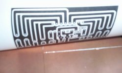
Hi teemuk,
No, I know what you are trying to do, most magazines publish PCB's which look like that. Try this, print out that file, just like I posted it, look through the back side (white part of the paper), then you will be able to read the text. I am posting a photo of how you should put the layout to make the PCB.
Regards,
Werner
Attachments
- Status
- Not open for further replies.
- Home
- Amplifiers
- Chip Amps
- Pcb to Stereo Amp LM386