Hello all
What are the forum recommendations for PCB design software? I am interested in getting someone to make a 10pc each or so. I will have about 10 or so different PCB designs. Mostly simple tube pres or mixer channel strips
Thanks and regards
Randy
What are the forum recommendations for PCB design software? I am interested in getting someone to make a 10pc each or so. I will have about 10 or so different PCB designs. Mostly simple tube pres or mixer channel strips
Thanks and regards
Randy
The best pcb program is the one you know how to use, but here are a couple of excellent, multi-platform free programs.
Be aware that the learning curve for most such programs is rather steep.
https://diptrace.com/
https://www.kicad.org/
Be aware that the learning curve for most such programs is rather steep.
https://diptrace.com/
https://www.kicad.org/
Last edited:

EasyEDA is online (can also be downloaded), free and is fairly easy to pick up for beginners.
It isn't as fully featured as say Kicad or Altium, but the libraries are fairly well stocked and it does the job just fine without such a steep learning curve.
It isn't as fully featured as say Kicad or Altium, but the libraries are fairly well stocked and it does the job just fine without such a steep learning curve.
Besides the excellent software suggested above, I suggest that, as practice,and to get into the proper mindframe, you start drawing simple PCBs "by hand"
Place the components on a large sheet of paper, well separated so as to easily draw many traces between them, and start penciling pin to pin connections.
Have a good eraser handy, erase tracks you don´t like, reroute them better, etc. ; you´ll start "seeing" best paths, layout, etc.
Mind you, drawing "on screen" amounts to about the same, so you are acquiring useful skills beforehand.
Thanks for the tip, man. I think you will be glad to hear that I will be tackling this with a solid background in both paper technical drawing and computer aided graphics design. I was just right now drawing the general arrangement for my Home theatre all in one box with live input channels, so then I can start CNC, laser and print process for chassis partsBesides the excellent software suggested above, I suggest that, as practice,and to get into the proper mindframe, you start drawing simple PCBs "by hand"
Place the components on a large sheet of paper, well separated so as to easily draw many traces between them, and start penciling pin to pin connections.
Have a good eraser handy, erase tracks you don´t like, reroute them better, etc. ; you´ll start "seeing" best paths, layout, etc.
Mind you, drawing "on screen" amounts to about the same, so you are acquiring useful skills beforehand.
Today after 20 years I gave up Corel Draw for a no name drawing application that comes with LibreOffice. I didn't have my desk pc with Corel here, so installed Libre freeware on the laptop to see if I can get the GA drawn up. I didn't like Inkspace much. I seem to be able to do most things with Libre and not missing anything so far. Just to confirm this, I installed a new Corel draw trial. Tried to redraw the GA with this and was finding it clumsier. That's it, another very expensive software out of the window! LibreOffice draw is very good for even quite complicated drawings with very many layers
My workshop machines have arrived, and today I added another workbench to hold the machines. It's full steam ahead with a number of concurrent projects now, 🙂 Keep an eye out for a new project blog in instruments and amps section. The GA drawings I'll post there will show the ability LibreOffice Draw has very well. The project is very ambitious but a good fun project to test some ideas. I need to draw some channel strip PCBs with that, which I hope to be able to order populated with SMD knobery and switchery to remove the chore of knob fitting and such for maybe over 8 channels
Thanks and regards
Randy
I have mixed feelings about that. Maybe it is a good place to start. You'll likely be able to see when swapping between the two opamps in a dual opamp (or the various gates in a logic IC) will help you get a good flow in the layout. Then again, I find the rats nest in a PCB layout tool to be very telling of the same thing.Besides the excellent software suggested above, I suggest that, as practice,and to get into the proper mindframe, you start drawing simple PCBs "by hand"
Place the components on a large sheet of paper, well separated so as to easily draw many traces between them, and start penciling pin to pin connections.
Have a good eraser handy, erase tracks you don´t like, reroute them better, etc. ; you´ll start "seeing" best paths, layout, etc.
I have only praise for the new version of KiCAD (version 6.0). I wasn't a fan of the older versions. I tried version 5.x and found the UI very 1990s Solaris-like. The UI was completely redone for version 6.0 and it is a joy to use. It seems like a mature piece of software. Sure. It has a few quirks, but so does any tool - even the expensive ones (2-3 different methods for opening a file that give different results in Altium for example).
I highly recommend the following workflow:
1) Draw the schematic. Select the proper PCB footprint for each component. Define footprints and symbols for any component that you use that's not in the KiCAD libraries.
2) Once the schematic is done, link it to the layout tool. This loads all the footprints into the PCB layout and shows the rats nest (i.e., all the connections you need to make between pins). KiCAD just throws all the parts right next to each other, which can be a bit overwhelming.
3) Place the footprints such that you get a clean layout. This is worth spending some time on. I usually start by organizing the components in functional groups. I then rotate and place the components within each functional group such that the group has a clean layout. Then bring the groups together. I find it helpful to do this in a few sittings. I often find that I can make improvements in the layout following a good night's sleep.
4) Draw the ground plane (if applicable). Then route the board. Route the critical signals first. Then power. Then everything else. As with the component placement, layout improvements can often be found after a good night's sleep.
5) Don't forget to add mechanical features such as mounting holes.
6) Run DRC (design rule check) and LVS (layout vs schematic). This ensures that the board is manufacturable and matches the schematic.
7) Double-check everything. Export Gerber files and send them off to the fab.
I'm not saying this is the correct workflow or the only workflow, just that it's a flow that's worked for me for decades. The most important thing is that you start with the schematic. It's much easier to find mistakes in the schematic than it is in the layout. So if the schematic is good and the layout passes LVS, the layout is good also (assuming the footprints are defined correctly anyway).
Tom
Excellent startup guide, thanks for that man. Seems like a good workflow that I start off withI have mixed feelings about that. Maybe it is a good place to start. You'll likely be able to see when swapping between the two opamps in a dual opamp (or the various gates in a logic IC) will help you get a good flow in the layout. Then again, I find the rats nest in a PCB layout tool to be very telling of the same thing.
I have only praise for the new version of KiCAD (version 6.0). I wasn't a fan of the older versions. I tried version 5.x and found the UI very 1990s Solaris-like. The UI was completely redone for version 6.0 and it is a joy to use. It seems like a mature piece of software. Sure. It has a few quirks, but so does any tool - even the expensive ones (2-3 different methods for opening a file that give different results in Altium for example).
I highly recommend the following workflow:
1) Draw the schematic. Select the proper PCB footprint for each component. Define footprints and symbols for any component that you use that's not in the KiCAD libraries.
2) Once the schematic is done, link it to the layout tool. This loads all the footprints into the PCB layout and shows the rats nest (i.e., all the connections you need to make between pins). KiCAD just throws all the parts right next to each other, which can be a bit overwhelming.
3) Place the footprints such that you get a clean layout. This is worth spending some time on. I usually start by organizing the components in functional groups. I then rotate and place the components within each functional group such that the group has a clean layout. Then bring the groups together. I find it helpful to do this in a few sittings. I often find that I can make improvements in the layout following a good night's sleep.
4) Draw the ground plane (if applicable). Then route the board. Route the critical signals first. Then power. Then everything else. As with the component placement, layout improvements can often be found after a good night's sleep.
5) Don't forget to add mechanical features such as mounting holes.
6) Run DRC (design rule check) and LVS (layout vs schematic). This ensures that the board is manufacturable and matches the schematic.
7) Double-check everything. Export Gerber files and send them off to the fab.
I'm not saying this is the correct workflow or the only workflow, just that it's a flow that's worked for me for decades. The most important thing is that you start with the schematic. It's much easier to find mistakes in the schematic than it is in the layout. So if the schematic is good and the layout passes LVS, the layout is good also (assuming the footprints are defined correctly anyway).
Tom
Until yet i am using the free designspark.
Attachments
-
 9AAEC27F-37BF-4D83-8C95-8DA2AD45EA4B.png11.1 KB · Views: 225
 -
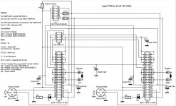 EDA17521-D893-4A31-A237-655BB3BD722A.jpeg277.6 KB · Views: 218
 -
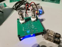 965E4F79-DD15-4A91-9C11-27E04C94AB59.jpeg462.6 KB · Views: 223
 -
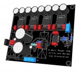 144596CA-C842-4BD2-BA76-3E14268EF5AD.jpeg145 KB · Views: 216
 -
 A0E356E5-2C87-456E-B60B-BA16B8DECC88.jpeg221.8 KB · Views: 233
 -
 2FAA388B-DFBA-480A-8BD3-87576BCE7507.jpeg156.7 KB · Views: 235
 -
 IMG_20220625_204443.jpg302.9 KB · Views: 214
 -
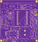
 1ET400A NC500 Tube preamp 3D.jpg183 KB · Views: 237
If you´re layouting high voltages, it would be nice to have a constraints feature for creepage and so.
Forward and backannotation (from schematics to layout and vice-versa) is the most important feature.
A PCB tool offering a big library is a plus.
And please, before routing, spend your time for correct components placement.
JP
Forward and backannotation (from schematics to layout and vice-versa) is the most important feature.
A PCB tool offering a big library is a plus.
And please, before routing, spend your time for correct components placement.
JP
(assuming the footprints are defined correctly anyway) THAT is a big one that I fouled up on earlier
this summer. I used the pin numbering of a different package of the same chip. I was trying to get
around the chip shortage and while I found a different package, I did not notice (MY FAULT) the pin
numbering was changed for THAT package. The bad board is stuffed and the chip error is bypassed
so when testing on the rest is complete, I will get the send the latest. I'm using KiCad 6 and agree
with Tom. MY problem is updating the libraries but Ultralibrarian and Component Search Engine (and
others) do much of the tedious work for you. I try to make schematic symbols the same as the
manufacturers data sheet and the Ultralibrarian parts are NOT that way, just a 'box with pins' but if
that is OK with you, no more work is needed. WAY back in the day I used Tango and while a DOS tool,
I could fly with it but I had to make MANY parts schematic and footprints which was a chore but pretty
easy to do. If you get "religious" about verifying symbols and footprints you'll have no problems. Don't
be afraid of 4 or more layers. I did lots in Tango and 4 so far in KiCad. The Chinese board houses like
JLCPCB (highly recommended) charge so little extra for 4 vs 2 layers it's silly NOT to use 4 layers.
G²
In desgnspark you can update/edit any footprint or symbol anytime. It has a large library. Missing parts are easy found at snapeda in the right format. You can easy make PCB without making the schematic first. Generate right on gerberfiles for PCB producer or make pdf 1:1 for making your own PCB’s
I learned this one last year, took me about 3 hrs to learn it.EasyEDA is online (can also be downloaded), free and is fairly easy to pick up for beginners.
It isn't as fully featured as say Kicad or Altium, but the libraries are fairly well stocked and it does the job just fine without such a steep learning curve.
Its open source so you can find some older footprints. Beware, some might not be accurate so double check them. What I like about it is you can use the web based software and use it anywhere. The auto routing works pretty good but I end up tweaking it some what. Adding a ground plane is a piece of cake.
I 2nd Kicad. It's super easy to use and I know a few electrical engineers who have started using it professionally.
Here's a good tutorial. It's old, so some things don't work quite like they did when the video was made.
Here's a good tutorial. It's old, so some things don't work quite like they did when the video was made.
I have been using my tools for IC design to create an input file for the open source program pcb and then output to gerber. If anyone comes from an IC background and wants to try it send me a PM. I'll toss you a license for my stuff. IC seems to be a very different style of design from PCB. Only Linux is supported, so it could also be IC is more *NIX style whereas I think PCB is more windows.
This is completely true. I personally know Altium better than any other program since I've been using it at work for years, but it's crazy expensive. For personal projects, I've been switching between KiCad and Eagle. Of the two, I prefer KiCad and would recommend it for most people.The best pcb program is the one you know how to use,
That's not a good workflow, though. It's way too easy to make a routing mistake that way. And you'll route from a schematic anyway so why not just draw it in the CAD tool so you have access to forward/back annotation, LVS, etc.?In desgnspark [...] You can easy make PCB without making the schematic first.
Tom
I find IC layout to be more three dimensional than PCB layout. I love how you can stack connectivity over devices in IC layout for example. Buried vias are free.IC seems to be a very different style of design from PCB.
True, though KiCAD is available for Windoze, *NIX, and MacOS. I especially appreciate the latter.Only Linux is supported, so it could also be IC is more *NIX style whereas I think PCB is more windows.
Tom
- Home
- Design & Build
- Software Tools
- PCB design tool?