The risk with something like Flux, is that one of the high end players will buy them to capture the user base, as happened to Eagle
FYI. right now if you design a PCB in EasyEDA, JLCPCB will give you an 8$ coupon to use. This means if you choose the cheapest shipping method, you can get 5 100x100 boards made and shipped for free.
got to like jlcpcb for protos and small runs.
- 2022-10-18 16:21:14
Order submitted
Your order has been submitted, waiting for payment now. - 2022-10-30 21:29:46
In Transit
2022/10/31 09:29:46 delivered to your community mailbox,
There are loads of different free PCBCAD packages now.
I wrote my own.
I can add any feature I like.
I added some auto placing functions.
There is a swap auto placer which switches around same type of components to find shortest net length sum.
I have recursive route and auto place which tries different component layouts and then routes them until it finds best route combination.
I added in very comprehensive design rule checking. From clearance, unused pin scan, max layer check etc etc
I have had over 350 different designs made buy JLCPCB and not found any major bugs.
Before anyone asks no I wont supply software name so as not to spam the group.

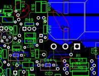
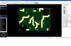
There is a pull down menu item, top menu bar, far right, where you select which layer you are working on. It is highlighted in the picture I attached. Diptrace is great. Very easy to use and very easy to order boards from directly in the tool without manually generating any files.Hi guys. Tell me how to edit the conductors on the other side in Diptrace. When they are transferred to the reverse side, they cannot be edited.
Attachments
I have struggled with a trail of old projects on Protel and Cadstar, where the original software licences are long lost when people left or PCs died.
You learn the importance of keeping all files as human readable ascii as KiCad does.
Undocumented binary files are vendor lock in.
For similar reasons, I would avoid cloud based design like the plague.
You learn the importance of keeping all files as human readable ascii as KiCad does.
Undocumented binary files are vendor lock in.
For similar reasons, I would avoid cloud based design like the plague.
I am wanting to design and have made a few small PCBs to hold a "ground breaker" circuit. You know, a small cap, two anti-phase diodes and a resistor but I don't know where to jump in. I don't know even the basics such as board thickness, trace specs, how many planes etc. I want to begin learning a bit about PCB design and this seems an easy place to get on board. I do stuff in DIY Layout like lay out schematics with parts.
I've looked at some of the online tools but they seem way to advanced for my need.
I've looked at some of the online tools but they seem way to advanced for my need.
I use KiCad if getting boards from a FAB. Otherwise, I use VeroRoute and stripboards. Stripboards provide a certain structure which gives a neater outcome than trial-and-error freestyle. Get VeroRoute from https://sourceforge.net/projects/veroroute/. There are examples in the DIY contruction tips forum.
These days with pc's with vast memory its fine to use ascii files.I have struggled with a trail of old projects on Protel and Cadstar, where the original software licences are long lost when people left or PCs died.
You learn the importance of keeping all files as human readable ascii as KiCad does.
Undocumented binary files are vendor lock in.
For similar reasons, I would avoid cloud based design like the plague.
In my early days a pc had 512k if you were lucky so data was then packed into bits and bytes and so hard to read back if you didnt have a key.
You could get 8 flags from a byte.
It's official, autodesk just killed Eagle, ending support in 2026. And their suggestion is to use Fusion, with a cost that is at least an order of magnitude higher...
So I am another refugee. Too bad, because I had my library fine tuned to fit my soldering style.
I think I will revisit Kicad. I have to admit though, last time I used it (at least 5 years ago) was a bit disappointing, especially because of bad documentation.
So I am another refugee. Too bad, because I had my library fine tuned to fit my soldering style.
I think I will revisit Kicad. I have to admit though, last time I used it (at least 5 years ago) was a bit disappointing, especially because of bad documentation.
I saw that this morning. They suggest using the Fusion360 Personal instead, which is free, but that only allows 2 layers at 80x80mm which isn't attractive enough for me to switch from EasyEDA.
OK KiCad version 7 works much much better. My previous experience (a few years back) was abysmal (Although, it could be that I now have a much better understanding of the underlying semantics)
I managed to import eagle projects very easily, and even copy my custom parts into a KiCad library.
Now I just need to figure out the DRC rules and the CAM process for the fabs
I managed to import eagle projects very easily, and even copy my custom parts into a KiCad library.
Now I just need to figure out the DRC rules and the CAM process for the fabs
It still has some very non-intuitive presets though. Like the zoom behavior, or the grid system, origins etc
I just saw the Eagle announcement and feel fortunate my only exposure was a couple of hours of instruction that didn't stick.
A few decades back I used this service, though sparingly because it was about $60 for three smallish (under 3"x5") boards. The enticing part is the PCB layout software is really easy to use, if you know anything about PCBs, there's practically no learning curve. The bad part is the vendor lock-in and the cost. Since I last used it it appears they added schematic capture with tie-in to the layout program. They're still in business: https://www.expresspcb.com
I DID use some computer cad PCB in the 1980s, there was a minicomputer based system named Telesis (Telesys?), then there was a package for the IBM PC/XT, forget the name but I remember it cost $149.
It's only in recent weeks that I've been coming up to speed on Kicad. I wouldn't call it "easy" though I thought Autocad was a bit of a learning curve 30 years ago, and once I got used to it it felt easy enough. Kicad has a huge number of features, and of course they're all on by default, to help people not make mistakes in PCBs. I just discovered how to turn off the 'Spice model error' so it'll ignore the lack of spice models on parts. I'm a long-term LTspice user and I didn't even know Kicad includes a spice (or does it?). Is there a way to write out a Kicad schematic that LTspice can read? The oddest KIcad thing I've seen so far was a SOIC TL074 with a 16-pin footprint with a couple of missing pads. I was able to reassign a 14-pin footprint to it easily enough.
Tom's comments about a structured (to use a programming buzzword from the 1970s/1980s) approach is well taken. I've known C for decades and learned a lot of C++ in the last decade, and keeping things organized becomes essential for large programming projects (and most anything useful becomes large). I think one thing circuit schematics should always have is an English (or whatever your language is) text description, even justifying use of most parts, as in the "Circuit Description" section of most Heathkit assembly manuals.
Here's a video series I followed and found helpful - but for most any of these, you have to watch all of every video, because even though the presenter goes over a lot of stuff "everyone knows," every video shows little Kicad details that are hard to find/learn any other way. I won't say this is the best Kicad video series, it might not even be better than average, but it helped me get over several "what do I do now" humps:
(edited to put in correct video)
I really need to keep making PCBs, just so I don't forget all this stuff I'm learning about Kicad ...
A few decades back I used this service, though sparingly because it was about $60 for three smallish (under 3"x5") boards. The enticing part is the PCB layout software is really easy to use, if you know anything about PCBs, there's practically no learning curve. The bad part is the vendor lock-in and the cost. Since I last used it it appears they added schematic capture with tie-in to the layout program. They're still in business: https://www.expresspcb.com
I DID use some computer cad PCB in the 1980s, there was a minicomputer based system named Telesis (Telesys?), then there was a package for the IBM PC/XT, forget the name but I remember it cost $149.
It's only in recent weeks that I've been coming up to speed on Kicad. I wouldn't call it "easy" though I thought Autocad was a bit of a learning curve 30 years ago, and once I got used to it it felt easy enough. Kicad has a huge number of features, and of course they're all on by default, to help people not make mistakes in PCBs. I just discovered how to turn off the 'Spice model error' so it'll ignore the lack of spice models on parts. I'm a long-term LTspice user and I didn't even know Kicad includes a spice (or does it?). Is there a way to write out a Kicad schematic that LTspice can read? The oddest KIcad thing I've seen so far was a SOIC TL074 with a 16-pin footprint with a couple of missing pads. I was able to reassign a 14-pin footprint to it easily enough.
Tom's comments about a structured (to use a programming buzzword from the 1970s/1980s) approach is well taken. I've known C for decades and learned a lot of C++ in the last decade, and keeping things organized becomes essential for large programming projects (and most anything useful becomes large). I think one thing circuit schematics should always have is an English (or whatever your language is) text description, even justifying use of most parts, as in the "Circuit Description" section of most Heathkit assembly manuals.
Here's a video series I followed and found helpful - but for most any of these, you have to watch all of every video, because even though the presenter goes over a lot of stuff "everyone knows," every video shows little Kicad details that are hard to find/learn any other way. I won't say this is the best Kicad video series, it might not even be better than average, but it helped me get over several "what do I do now" humps:
(edited to put in correct video)
I just tried adding a TL074 to a test schematic and there is no pre-assigned footprint.The oddest KIcad thing I've seen so far was a SOIC TL074 with a 16-pin footprint with a couple of missing pads
The pin count filter correctly allows you to choose a 14 pin SOIC and it is definitely a 14 pad footprint
My pcbcad software has a "swap auto placer" which swaps same type components until shortest net is found.Besides the excellent software suggested above, I suggest that, as practice,and to get into the proper mindframe, you start drawing simple PCBs "by hand"
Place the components on a large sheet of paper, well separated so as to easily draw many traces between them, and start penciling pin to pin connections.
Have a good eraser handy, erase tracks you don´t like, reroute them better, etc. ; you´ll start "seeing" best paths, layout, etc.
Mind you, drawing "on screen" amounts to about the same, so you are acquiring useful skills beforehand.
Got me out of trouble a few times with difficult to route pcb's.
Having no preassigned footprint means you can use the foot print you want without having 10 different versions of same component with different footprints.I just tried adding a TL074 to a test schematic and there is no pre-assigned footprint.
The pin count filter correctly allows you to choose a 14 pin SOIC and it is definitely a 14 pad footprint
- Home
- Design & Build
- Software Tools
- PCB design tool?