I haven't tried EasyEDA mostly because I don't particularly like online tools in general. I prefer to work offline. But EasyEDA does have two versions of a "desktop client" ("Professional" and "Standard"). Has anyone used the desktop applications? Do they have limitations compared to the online versions?
Diptrace has a very good user interface and you can order boards with the press of a button from either California or China. There is no fiddling around with getting the correct type of drawing sent to a PCB house. The prices from PCBWay are very good. It is easy to swap between the schematic and layout as well. The auto route function works well, as you can specify a small set of traces to be routed at a time.
I had very high hopes on Diptrace, used it for a while (part as my main routine), looked so very promising.Diptrace has a very good user interface and you can order boards with the press of a button from either California or China. There is no fiddling around with getting the correct type of drawing sent to a PCB house. The prices from PCBWay are very good. It is easy to swap between the schematic and layout as well. The auto route function works well, as you can specify a small set of traces to be routed at a time.
Unfortunately their improvements seem to have stalled heavily the last few years.
In my search for an easy-to-use program to replace the now unsupported one I have been using, I came across LibrePCB:
https://librepcb.org/
The product description acknowledges that it is not as mature as KiCad (it hasn't yet reached version 1.0). But as a hobbyist I doubt that I will ever need the sophistication of either KiCad or DipTrace. Does anyone have any experience with LibrePCB?
https://librepcb.org/
The product description acknowledges that it is not as mature as KiCad (it hasn't yet reached version 1.0). But as a hobbyist I doubt that I will ever need the sophistication of either KiCad or DipTrace. Does anyone have any experience with LibrePCB?
Regardless of of the EDA package that you choose, please, please, please spend the time to carefully organize and lay out your schematic. I know that everyone has his or her own special way to layout a PCB and that's great. However, if your schematic is difficult to decipher, it makes for a whole lot of headaches down the road. I see this at work all the time with our legacy designs and it sucks to deal with.
For a moderate to highly complex design, consider using a hierarchical approach to the schematic and spread the design over several schematic sheets. That is, if your EDA package supports it. Do not pack everything onto one page, just to have everything on one page. It can make the design difficult to debug, and even more difficult to understand when you have to go back to it a year or two later because you don't like something and want to make a second revision. It also makes it challenging to review or share - especially if you're the reviewer and not the draftsman!
For a moderate to highly complex design, consider using a hierarchical approach to the schematic and spread the design over several schematic sheets. That is, if your EDA package supports it. Do not pack everything onto one page, just to have everything on one page. It can make the design difficult to debug, and even more difficult to understand when you have to go back to it a year or two later because you don't like something and want to make a second revision. It also makes it challenging to review or share - especially if you're the reviewer and not the draftsman!

Member
Joined 2009
Paid Member
Interesting thread, good to hear other experiences. I started with and used Eagle for at least a decade, the free hobbyist version. No complaints about it in general, the only thing I didn’t enjoy was making and adding new parts if they weren’t in the library. The free version will limit future projects and they no longer offer anything affordable so I’ve dropped the idea to use them. I’ve downloaded KiCad6 after reading about the big improvements made by very skilled people finding extra time during the pandemic. I expect a steep learning curve so hopefully no nasty surprises. I use a Mac.
I started making PCB's as a kid with masking tape, an X-Acto knife and some Ferric Chloride from the Lafayette Radio Electronics store. We didn't have a Radio Shack. I graduated to Bishop Graphics tape and patterns on Mylar in the 70's. The 4:1 mylar was reduced using a darkroom enlarger as a camera, then exposed on to Kodalith litho film with the same enlarger at 1:1 size. The Litho film was then used to expose the photo sensitive PCB material using a UV light. I did a couple PC boards for the SS-50 bus computer system from SWTPC in the late 70's and many other projects through the 80's.
My first venture into CAD tools was Eagle 2.6 on DOS running on a 486 based PC in 1992 or 1993. I still use Eagle 5.11 for my vacuum tube based boards. When Cadsoft was acquired by Newark / Farnell the cost of upgrading to V6.x was over $600, which turned into an expensive yearly lease when Autodesk took over. Tube amp PC boards are usually large enough to require the pro version, so I'm still on Eagle 5.11.
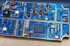
I did PC boards at Motorola on Mentor Graphics tools for about 20 years until they decided to switch to Cadence. I did exactly one board in the Cadence system before retiring in 2014. It is the RF deck for a two way radio prototype and is seen here. There are over 600 components on a board roughly 6 square inches in size. This board is a 10 layer 2-6-2 HDI board. High Density Interconnect technology uses a conventional board in the middle (6 layers in this case) and two (in this case) or more layers of what is essentially photomask with laser drilled holes for high density routing for the outer layers. This is often the only way to route to every pin on a small BGA chip with say 144 balls. The purpose of this board was to evaluate the super secret custom CMOS RF chip that our group designed in a real working two way radio. The chip it the one with no markings in the center of the first photo. Another chip was developed after I retired to replace the hybrid modules in the brass cans and their controller chip. This technology is now a full fledged product.
As I restarted my experimenting with music synthesizer stuff, I have been looking at different PCB tools, and have tentatively settled on Kicad 6, but I have yet to complete a board with it.
I tend to agree with tomchr's workflow for two reasons. It was enforced at Motorola, for anything that might ever make it into a product. Since I only did prototypes, I could bend the rules, and I did make some simple RF test boards without schematics. There was always the possibility that my project could get handed off to someone else, so proper protocol was the path of least resistance. I learned to follow it on my home projects even if it sometimes meant doing the schematic twice, once in LT spice, then again for Eagle. There was a period of time when I was stuck in a car, doctors office, airplane, or wherever, so I used that time to turn Dumm Blonde Ideas into schematics, LT spice sims, and PC board layouts. The Tubelab Universal Driver board was an idea that happened in 2007 or 2008. It wound up in Eagle and LT Spice where it slept quietly on a hard drive until 2014 when I made one and tested it out. Having three levels of documentation instead of just a PCB layout was key to being able to reawaken the thoughts that created the board in the first place 6 years prior. Now if I only was so OCD with my Teensy (like an Arduino) code, I could understand the working music synthesizer I built 5 years ago. I look at my code and ask myself, "I wrote this, really? How does it work?"
My first venture into CAD tools was Eagle 2.6 on DOS running on a 486 based PC in 1992 or 1993. I still use Eagle 5.11 for my vacuum tube based boards. When Cadsoft was acquired by Newark / Farnell the cost of upgrading to V6.x was over $600, which turned into an expensive yearly lease when Autodesk took over. Tube amp PC boards are usually large enough to require the pro version, so I'm still on Eagle 5.11.
I did PC boards at Motorola on Mentor Graphics tools for about 20 years until they decided to switch to Cadence. I did exactly one board in the Cadence system before retiring in 2014. It is the RF deck for a two way radio prototype and is seen here. There are over 600 components on a board roughly 6 square inches in size. This board is a 10 layer 2-6-2 HDI board. High Density Interconnect technology uses a conventional board in the middle (6 layers in this case) and two (in this case) or more layers of what is essentially photomask with laser drilled holes for high density routing for the outer layers. This is often the only way to route to every pin on a small BGA chip with say 144 balls. The purpose of this board was to evaluate the super secret custom CMOS RF chip that our group designed in a real working two way radio. The chip it the one with no markings in the center of the first photo. Another chip was developed after I retired to replace the hybrid modules in the brass cans and their controller chip. This technology is now a full fledged product.
As I restarted my experimenting with music synthesizer stuff, I have been looking at different PCB tools, and have tentatively settled on Kicad 6, but I have yet to complete a board with it.
I tend to agree with tomchr's workflow for two reasons. It was enforced at Motorola, for anything that might ever make it into a product. Since I only did prototypes, I could bend the rules, and I did make some simple RF test boards without schematics. There was always the possibility that my project could get handed off to someone else, so proper protocol was the path of least resistance. I learned to follow it on my home projects even if it sometimes meant doing the schematic twice, once in LT spice, then again for Eagle. There was a period of time when I was stuck in a car, doctors office, airplane, or wherever, so I used that time to turn Dumm Blonde Ideas into schematics, LT spice sims, and PC board layouts. The Tubelab Universal Driver board was an idea that happened in 2007 or 2008. It wound up in Eagle and LT Spice where it slept quietly on a hard drive until 2014 when I made one and tested it out. Having three levels of documentation instead of just a PCB layout was key to being able to reawaken the thoughts that created the board in the first place 6 years prior. Now if I only was so OCD with my Teensy (like an Arduino) code, I could understand the working music synthesizer I built 5 years ago. I look at my code and ask myself, "I wrote this, really? How does it work?"
Attachments
Very easy, best 49 bucks I've ever spent. I use sprint-layout to design the board usually in one relaxing evening, two clicks to export it, upload it to jlcpcb, and in 5-7 days the boards are on my doorstep! I also like to make all my own footprints, once I have the components in hand and my micrometer caliper to get exact footprints faster than hunting down the mfg footprints. I can relax the hole sizes, etc. make exact tube socket pads etc. I would suggest a draw it yourself program over bothering with auto-routing and having to first enter your schematic, too time consuming for me. I just print the schematic and have fun drawing the board, routing out shapes, board shape, doing edge card pins, its all been very easy.
https://www.electronic-software-shop.com/lng/en/sprint-layout-60.html?language=en
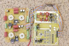
Here is my latest, a power supply LCRC (to split LCLC stereo) filter train that uses DC link capacitors, vacuum tube rectifier with socket over an open hole, on board quasimodo snubbers, on-board heater elevation voltage divider reference, fuses to protest the power transformer secondary, bleeder resister, etc.
Bottom side (note tube rectifier mounts on this side over the open hole and oval mounting screws for saddle) it will accept octal or 9 pin rectifier, I managed to do this board with only two traces needed to go on the top side to do a hop:

Top side

https://www.electronic-software-shop.com/lng/en/sprint-layout-60.html?language=en
Here is my latest, a power supply LCRC (to split LCLC stereo) filter train that uses DC link capacitors, vacuum tube rectifier with socket over an open hole, on board quasimodo snubbers, on-board heater elevation voltage divider reference, fuses to protest the power transformer secondary, bleeder resister, etc.
Bottom side (note tube rectifier mounts on this side over the open hole and oval mounting screws for saddle) it will accept octal or 9 pin rectifier, I managed to do this board with only two traces needed to go on the top side to do a hop:
Top side
Last edited:
I didn't find the learning curve to be that steep. I'd start with a "getting started" video and then google when you get stuck. I found plenty of help was available.I’ve downloaded KiCad6 after reading about the big improvements made by very skilled people finding extra time during the pandemic. I expect a steep learning curve so hopefully no nasty surprises. I use a Mac.
Tom
Yes, they did have some issues with the auto-routing a few months back but its resolved.Here in the Netherlands very stable connection(1Gb/s). Easy Eda server had then a lot of problems. May be it is nowadays better.
Sometimes you need to save your work and refresh it before you do the routing
Professionals would not use an outdated version of pcb software. That is very risky to say the least.
Eagle is only worthwhile if you already know how to use it. Otherwise, the other programs mentioned here are better.
Eagle is only worthwhile if you already know how to use it. Otherwise, the other programs mentioned here are better.
Last edited:
I have used Eagle for DOS in my non Motorola contract engineering jobs dating back to the early 90's. I still use the 2010 vintage version 5.11 for the reasons I previously stated. Other than the lack of library parts (5.11 will not read anything from 6.0 on) It works fine in W10 and does not pose any known risks. Most of my work has involved PC boards with unique parts where I need to make my own library parts anyway, so that hasn't been a big issue.Professionals would not use an outdated version of pcb software. That is very risky to say the least.
Eagle is only worthwhile if you already know how to use it. Otherwise, the other programs mentioned here are better.
Part of the reason for sticking with Eagle is similar to the reason I was one of the last Mentor Graphics users at Motorola. After using something for almost 30 years and learning how to make it do what I want, it's hard to change, but I do agree that today's version of Eagle with its user requirements and yearly license fee would not be something I would even consider.
I have Kicad 6 on this PC and have played with it a bit, but I haven't actually finished a board yet. There is no rush to finish it since I can't get the chips to build it.
I do the same (use an old and now unsupported program), but I've been thinking about moving on to a modern PCB application that can be expected to be around for a long time to come. But it's hard to part with an application that I'm so familiar with, and as long as the work products that I deliver to consulting clients are just the Gerber files and not the PCB application source files, I suppose I can continue doing what I'm doing for now.
CERN supports KiCad, so that's the one free program with a guaranteed future.
https://ohwr.org/project/cern-kicad/wikis/home
Professional level support is also available for an annual fee. The software is still free.
https://www.kipro-pcb.com/main/subscribe/
https://ohwr.org/project/cern-kicad/wikis/home
Professional level support is also available for an annual fee. The software is still free.
https://www.kipro-pcb.com/main/subscribe/
Last edited:
My deliverables have always been physical products, usually PC boards or design packages including Gerber files and some working prototypes. In a few cases I gave the customer the complete design but sold them the flashed secure microcontroller on a continuous basis. All were done with Eagle or Bishop Graphics and a darkroom.I do the same (use an old and now unsupported program), but I've been thinking about moving on to a modern PCB application that can be expected to be around for a long time to come. But it's hard to part with an application that I'm so familiar with, and as long as the work products that I deliver to consulting clients are just the Gerber files and not the PCB application source files, I suppose I can continue doing what I'm doing for now.
Back in 2008 I submitted a complex electronic design to a contest that ran in Circuit Cellar magazine. It involved a single ended vacuum tube audio amplifier with a modulated high voltage power supply all controlled by a Microchip dsPIC chip for a serious improvement in operating efficiency. This won a prize in the contest and a published article in the magazine. These concepts were taken from some high efficiency RF amplifier work I was doing at the time and were largely ignored or shunned by the vacuum tube amp aficionados.
There were two PC boards in the design, one contained all of the vacuum tube circuitry while the other contained the low voltage opamps, microcontroller and isolated modulated power supply needed to transform a class A SET into a class H SET. Both were done using Eagle in 2007. I have recently awakened these boards from a 15 year sleep in a closed cardboard box for a possible redesign using more a modern and powerful controller paired with one of my newer SE amp designs.
It would be easiest to do the tube amp board in Eagle since I have several existing designs to start from. The digital board is a different story which will likely be a learning experience for Kicad or possibly another tool if I hit a roadblock.
Attachments
If you want a modern cloud-based thing, there's https://www.flux.ai
I've used their schematic capture and found it pretty nice and easy to use, but I haven't tried their PCB layout yet, but they do support it.
I've used their schematic capture and found it pretty nice and easy to use, but I haven't tried their PCB layout yet, but they do support it.
- Home
- Design & Build
- Software Tools
- PCB design tool?