One of my first PCBs was totally by hand as it was designed BC (before computers). It is WAY tooThat's not a good workflow, though. It's way too easy to make a routing mistake that way. And you'll route from a schematic anyway so why not just draw it in the CAD tool so you have access to forward/back annotation, LVS, etc.?
Tom
easy to make a mistake and not see it. You just decide it is right and keep missing it. I swore I
would never do another PCB because it's too intense to keep everything straight without someone
else to double check. Then I got Tango in '89 and tried another board. A netlist is your best friend
along with clearance checks then renumbering so it can be assembled by a human. I partly automated
it in Tango and could manually renumber a board of 950 parts by lunch. KiCad 6 now includes
renumbering that takes seconds.
Your workflow encourages no mistakes and if you do, it's a LOT easier to get the next revision out.
G²
Oh, sure. If you would rather create a netlist than a schematic that's fine. As long as you're not going directly from a napkin drawing to the PCB... In "The Good Old Days", the flow was: Schematic->Netlist->PCB. Modern tools just hide the netlist and make it a one-step process to import the schematic into the PCB tool.
I've made some 'BC' PCB layouts too. I drew my first board by hand with a DALO pen and etched it in ferric chloride. Then drilled it with a plain power drill in a drill stand. I operated like that for a few years before starting PCB layout on computers. In those days I had paper schematics and drew the PCBs without a netlist. I'm all too familiar with seeing but not seeing mistakes. 🙂
It turns out I missed a step in my recommended flow. Here's the full flow with that step added:
1) Draw the schematic. Select the proper PCB footprint for each component. Define footprints and symbols for any component that you use that's not in the KiCAD libraries.
2) Once the schematic is done, link it to the layout tool. This loads all the footprints into the PCB layout and shows the rats nest (i.e., all the connections you need to make between pins). KiCAD just throws all the parts right next to each other, which can be a bit overwhelming.
3) Place the footprints such that you get a clean layout. This is worth spending some time on. I usually start by organizing the components in functional groups. I then rotate and place the components within each functional group such that the group has a clean layout. Then bring the groups together. I find it helpful to do this in a few sittings. I often find that I can make improvements in the layout following a good night's sleep.
4) Draw the ground plane (if applicable). Then route the board. Route the critical signals first. Then power. Then everything else. As with the component placement, layout improvements can often be found after a good night's sleep.
5) Don't forget to add mechanical features such as mounting holes.
6a) One of the quirks in KiCAD is that it's a bit too easy to leave little trace stubs here and there, often hidden under pads. It has a script to remove those automatically, so I run that after the layout is complete.
6b) Run an automated check for un-routed nets. Do NOT rely on a visual inspection for this as it's way too easy to miss a short, unconnected net somewhere (ask me how I know!)
7) Run DRC (design rule check) and LVS (layout vs schematic). This ensures that the board is manufacturable and matches the schematic.
8) Double-check everything. Export Gerber files and send them off to the fab.
I should also mention that the board should be DRC clean. I.e., all design rules passed with no violations. Before KiCAD the tool I used did not like vias under components, so all the thermal vias would get flagged with DRC errors. In that case, I would have, say, 16 DRC violations. "No big deal", you say. Just remember check that it's 16 DRC errors every time you run the DRC. The trouble with that is that it's way too easy to miss when 16 turns to 18 due to two 'real' violations, and now you have a PCB layout that can't be manufactured or - even worse - that arrives from the fab with connections where you didn't want them.
I actually created a copy of the final layout where I deleted the thermal vias and made sure that layout was DRC clean before I submitted the layout to the fab. But, of course, that approach comes with a new set of risks. It's pretty easy to then either continue editing in the wrong file or submitting the wrong file to the fab.
I, thankfully, never got bit by this approach but it always made me a bit nervous. I know a few IC layout designers who've been bit by that sort of stuff. That gets really expensive in a hurry.
The LVS should be clean for fairly obvious reasons.
During the layout process I colour the nets for V+ red, V- blue, and ground green. It makes it easier to tell the power nets from the signal nets.
Some may find my process a bit anal, but there are few things I hate more than wasting my time or my money. A PCB layout that doesn't work wastes both.
Tom
Last edited:

The netlist I made was from Tango schematic. I've never created one by hand.
That sounds like a PCB with no schematic. Your process isn't anal (though I
prefer OCD). You found "gotchas" that need to be handled to learn from previous
errors. If you don't do that, you're doomed to more errors. I always tell my kids
to only make NEW mistakes.
Lest anyone think Tango was great, PCB program had binary or ASCII (text)
for the files. Binary mode would randomly lose a trace segment which got
me to frequently do a "Net verify" especially after exporting Gerbers, just to
be safe. Text files were larger but hardly a problem and were easy to run my
renumbering. All parts would get an X in front of the designator so C1 became
XC1, verify LVS, renumber by hand and back annotate into schematic. Worked
OK.
I only do 4 layers. That ground plane gets rid of lot of loop problems. The other
inner layer is for power and control lines that are known to be no chance of
errors. The outer layers are for parts, lately both sides to the point I have to
be careful with heat. 3.3V wastes least power as SMPS, basically those 3 term
replacements. Latest board would be 5-6 Watts with linears but less than 2 Watts
with switchers. 6 Watts in 100 cubic inches is a problem. 2 Watts is OK.
G²
I recently started using KiCad 6.0 after having used Eagle. Here is a simple example that fits in an Altoids tin for storage.Hello all
What are the forum recommendations for PCB design software
I sent the Gerber to JLCPCB. Five PCBs arrived a week later.
I usually make the PCB look like the schematic and then spend most of the time trying a couple of satisfactory layouts.
FunFact: If instead you are going to solder on a grid board, you can use KiCad to plan the layout.
Attachments


FunFact: If instead you are going to solder on a grid board, you can use KiCad to plan the layout.
If you then print out the board 1:1, you can tape it on the grid board, and push the component leads right through it.
That goes very fast. You can even have component numbers and values for stuffing. Works great.
Last edited:
You say this but I've been designing PCBs for years without schematics first in the PCB design software.Oh, sure. If you would rather create a netlist than a schematic that's fine. As long as you're not going directly from a napkin drawing to the PCB... In "The Good Old Days", the flow was: Schematic->Netlist->PCB. Modern tools just hide the netlist and make it a one-step process to import the schematic into the PCB tool.
I've made some 'BC' PCB layouts too. I drew my first board by hand with a DALO pen and etched it in ferric chloride. Then drilled it with a plain power drill in a drill stand. I operated like that for a few years before starting PCB layout on computers. In those days I had paper schematics and drew the PCBs without a netlist. I'm all too familiar with seeing but not seeing mistakes. 🙂
It turns out I missed a step in my recommended flow. Here's the full flow with that step added:
1) Draw the schematic. Select the proper PCB footprint for each component. Define footprints and symbols for any component that you use that's not in the KiCAD libraries.
2) Once the schematic is done, link it to the layout tool. This loads all the footprints into the PCB layout and shows the rats nest (i.e., all the connections you need to make between pins). KiCAD just throws all the parts right next to each other, which can be a bit overwhelming.
3) Place the footprints such that you get a clean layout. This is worth spending some time on. I usually start by organizing the components in functional groups. I then rotate and place the components within each functional group such that the group has a clean layout. Then bring the groups together. I find it helpful to do this in a few sittings. I often find that I can make improvements in the layout following a good night's sleep.
4) Draw the ground plane (if applicable). Then route the board. Route the critical signals first. Then power. Then everything else. As with the component placement, layout improvements can often be found after a good night's sleep.
5) Don't forget to add mechanical features such as mounting holes.
6a) One of the quirks in KiCAD is that it's a bit too easy to leave little trace stubs here and there, often hidden under pads. It has a script to remove those automatically, so I run that after the layout is complete.
6b) Run an automated check for un-routed nets. Do NOT rely on a visual inspection for this as it's way too easy to miss a short, unconnected net somewhere (ask me how I know!)
7) Run DRC (design rule check) and LVS (layout vs schematic). This ensures that the board is manufacturable and matches the schematic.
8) Double-check everything. Export Gerber files and send them off to the fab.
I should also mention that the board should be DRC clean. I.e., all design rules passed with no violations. Before KiCAD the tool I used did not like vias under components, so all the thermal vias would get flagged with DRC errors. In that case, I would have, say, 16 DRC violations. "No big deal", you say. Just remember check that it's 16 DRC errors every time you run the DRC. The trouble with that is that it's way too easy to miss when 16 turns to 18 due to two 'real' violations, and now you have a PCB layout that can't be manufactured or - even worse - that arrives from the fab with connections where you didn't want them.
I actually created a copy of the final layout where I deleted the thermal vias and made sure that layout was DRC clean before I submitted the layout to the fab. But, of course, that approach comes with a new set of risks. It's pretty easy to then either continue editing in the wrong file or submitting the wrong file to the fab.
I, thankfully, never got bit by this approach but it always made me a bit nervous. I know a few IC layout designers who've been bit by that sort of stuff. That gets really expensive in a hurry.
The LVS should be clean for fairly obvious reasons.
During the layout process I colour the nets for V+ red, V- blue, and ground green. It makes it easier to tell the power nets from the signal nets.
Some may find my process a bit anal, but there are few things I hate more than wasting my time or my money. A PCB layout that doesn't work wastes both.
Tom
You say you're going to make a schematic anyway... except I'm not for 99% of the stuff I create.
I print out my PCB designs, enlarged to the A4 sheet, and check them by hand Vs a datasheet schematic and/or device pinout prior to construction. Do I make mistakes? Sometimes but not often.
I hate drawing out schematics even in simulation software. Absolutely hate it.
I also use Designspark PCB. You don't have to use it without a schematic if you don't want to you just can.
Would have drawing the schematics out first have saved me time in the long run? No, quite the opposite. It would have wasted loads of it plus hating every step of it along the way. Pretty much all small errors I've made are easily correctable with a metal file/scalpel and very thin wire.
I suppose it goes without saying that, because almost everything I do is a prototype, I end up hacking the PCB to bits anyway because of a small design change I wish to make. Even if every PCB I made was schematic perfect from the start it would end up with some modification.
Have to agree, I do all my boards the same way, and it's much faster. Mistakes are very rare, but I'm careful.
I recently started using KiCad 6.0 after having used Eagle. Here is a simple example that fits in an Altoids tin for storage.
I sent the Gerber to JLCPCB. Five PCBs arrived a week later.
I usually make the PCB look like the schematic and then spend most of the time trying a couple of satisfactory layouts.
FunFact: If instead you are going to solder on a grid board, you can use KiCad to plan the layout.
Thank you two. Great tipsHave to agree, I do all my boards the same way, and it's much faster. Mistakes are very rare, but I'm careful.
And if you're willing to accept that and the resulting reliability issues, that's great. I'm not willing to accept that level of quality.Pretty much all small errors I've made are easily correctable with a metal file/scalpel and very thin wire.
I can draw a schematic pretty quickly. The laborious task is to get all the footprints selected and getting the BOM information entered. If you're creating your PCB layouts from a napkin drawing you still have to select footprints. Entering the BOM information is optional but saves me time later. I probably spend 5-6x the amount of time on the actual PCB layout, so the schematic entry amounts to maybe 15-20% of the time involved with a PCB layout. To me, that's a very worthwhile tradeoff.
But each to their own I guess. I prefer stuff that works the first time. But then I've also worked in environments where stuff was mass-produced and a screwup in the IC layout would cost a few years of my salary and a few months of project delay. I carry that same philosophy into my own work. I also try to let the tools work for me rather than the other way around.
Tom
Well I mean the reliability issues are minimal and over time I'd have wasted time in inputting schematics rather than saving it by not having had a couple of PCBs with issue. I also make the majority of my own PCBs myself so it's not weeks later for a design revision from China.And if you're willing to accept that and the resulting reliability issues, that's great. I'm not willing to accept that level of quality.
I can draw a schematic pretty quickly. The laborious task is to get all the footprints selected and getting the BOM information entered. If you're creating your PCB layouts from a napkin drawing you still have to select footprints. Entering the BOM information is optional but saves me time later. I probably spend 5-6x the amount of time on the actual PCB layout, so the schematic entry amounts to maybe 15-20% of the time involved with a PCB layout. To me, that's a very worthwhile tradeoff.
But each to their own I guess. I prefer stuff that works the first time. But then I've also worked in environments where stuff was mass-produced and a screwup in the IC layout would cost a few years of my salary and a few months of project delay. I carry that same philosophy into my own work. I also try to let the tools work for me rather than the other way around.
Tom
I agree that if this was for a company, where years worth of salary would be the cost of a PCB error, that I'd draw schematics but that's not the reality of my situation.
Footprints don't take me that long. Most are copy paste from previous ICs that use the same package and then there are repositories online that satisfy most of what I don't have. All I need is the correct package, for example I'll grab an online microcontroller footprint and use it for a power converter so long as they share the same package.
When going the schematic and PCB route how do footprints work? Do you need to rename every pin on the footprint to match the name of the pin in the schematic or is it all just numbers? If I had to rename every pin every time I wanted to duplicate a footprint that would take forever, and be error prone, what if you make a mistake drawing the schematic? Same with components I just have a generic 1206 footprint, for example, that I use for all 1206 objects, capacitors, resistors, inductors, etc none of them need naming, or linking, to a schematic component. It's just 1206. I don't use silk screens either so nothing needs a correct name.
The footprint is part of the schematic symbol. Any time you pull up a part you get<snip>
When going the schematic and PCB route how do footprints work? Do you need to rename every pin on the footprint to match the name of the pin in the schematic or is it all just numbers? If I had to rename every pin every time I wanted to duplicate a footprint that would take forever, and be error prone, what if you make a mistake drawing the schematic? Same with components I just have a generic 1206 footprint, for example, that I use for all 1206 objects, capacitors, resistors, inductors, etc none of them need naming, or linking, to a schematic component. It's just 1206. I don't use silk screens either so nothing needs a correct name.
the footprint. Some parts are available in DIP or SOIC or whatever so you HAVE to
pay attention to the suffix on the part to get the right pinout/footprint. Most of the
SMD passives I use are 0805 but may be 1206, 1210 etc. In Kicad the "symbol fields
table" groups the parts by value so you can change all the 100 Ohm resistors to
0603 and leave the rest alone. Silk screen makes assembling a lot easier by hand
if you have hundreds of parts - especially if the resistors and caps use the same footprint.
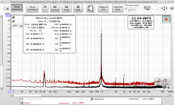
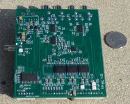
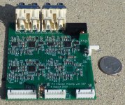
I added some pix of the latest project to get the idea of silk screen
G²
Attachments
I think you have two concepts conflated: Schematic symbols and footprints.Footprints don't take me that long. Most are copy paste from previous ICs that use the same package and then there are repositories online that satisfy most of what I don't have. All I need is the correct package, for example I'll grab an online microcontroller footprint and use it for a power converter so long as they share the same package.
When going the schematic and PCB route how do footprints work? Do you need to rename every pin on the footprint to match the name of the pin in the schematic or is it all just numbers?
Schematic symbols are really just graphics. They contain pins. Each pin can have properties (open collector, input, output, power, etc.) which is used for an electrical rules check at the schematic level. Pins also have names and numbers. The name is just for you. The number is what the CAD tools cares about.
Footprints define the part physically on the PCB. Footprints are generic (DIP-08, axial resistor with 0.4" pin spacing, etc.) and you can reuse the same footprint across many parts (assuming they fit in the same hole pattern in the PCB).
The parts on the schematic have a 'footprint' property field where you type (or copy-n-paste) the footprint name. As @stratus46 mentions above, the footprint can also be included when you define the symbol. This is pretty handy, in particular when there are multiple near-identical footprints (say SOICs with slight differences in their lengths or QFNs with slight differences in pin pitch and thermal pad size). I always add the footprint to any symbol that I draw. That way I know that I will get the correct footprint on the PCB when I pick a part from the library. That saves me time (and board spins) later.
I do a fair amount of copy-n-paste between schematics as well.
So when you import the schematic into the layout tool (or export the netlist in the old days) you basically tell the PCB layout tool that pin 1 of footprint U1 needs to connect to pin 2 of footprint U2 and so on. The PCB tool uses that information to draw a rat's nest of nets. I find the rat's nest pretty useful for component placement, actually. I find it easier to optimize the layout when I can immediately visualize the impact of parts rotation on the layout by how the rat's nest changes.
I agree that hobbyists don't necessarily need to follow the 'production' workflow that I suggest, but I would rather teach newcomers a solid workflow so they can let the tools work for them.
Tom
Last edited:
As a professional I have used all kinds of programs even programs like PADS. They all have their quirks and bugs, even Altium or Orcad. Btw Eagle now fully integrates with Fusion360.
To start with I would highly recommend EasyEDA. It's by far the easiest to understand. Plus a very big bonus is the enormous library they already have with parts, footprints and 3D models.
In fact, that saves so much time and hassle that I sometimes still use it for easier projects.
It's more than adequate for the vast majority of audio circuits.
Most of the time you don't have to draw any footprints at all!
It only does very poor when there are many different copper poors and different nets with different clearances for example. (Different clearances per pin or pad is not really possible).
But nothing you really need in general.
I am personally no fan at all of KiCad. It used to be so extremely inconsistent and messy. Issues with compatibility between updates (a no go if you want to use it a bit more seriously). They finally seem to solve that in the latest version.
I am also no fan of Eagle. The user interface doesn't feel intuitive to me at all. Even after all those years it still gets me.
But my biggest recommendation would be to just install and/or use a couple and see how it feels.
Because in the end it's more like a personal taste thing.
Ain't that the truth! I've used Protel Autotrax, OrCAD, and Altium along with some Cadence tools for IC design. All quirky. I find the quirks in KiCAD 6 are mostly in the schematic tool, which is where I spend the least amount of time. The layout tool is pretty competent. That said, I have only recently converted to KiCAD so it's possible I haven't pushed the tools much yet. I've yet to feel limited by the layout tool.They all have their quirks and bugs, even Altium or Orcad.
I did some testing in KiCAD 5.1 while 6.0 was still in beta. I had no issues with compatibility. I ended up using the beta version for a couple of layouts because it was so much better than 5.1. The only sorta kludge in the nightly releases of the beta version was that the Apple installer wasn't fully implemented so I had to delete and copy some files manually. Took five seconds. Oh no...! 🙂 That's fixed in the final release.I am personally no fan at all of KiCad. It used to be so extremely inconsistent and messy. Issues with compatibility between updates (a no go if you want to use it a bit more seriously). They finally seem to solve that in the latest version.
Me neither. Granted I last looked at Eagle 20+ years ago. It was pretty awful then. It looks like they now want real money for Eagle. I think I'd rather support the KiCAD project.I am also no fan of Eagle. The user interface doesn't feel intuitive to me at all. Even after all those years it still gets me.
Tom
You must have a poor connection, I have no problems using the online version.Easy Eda the online version has a lot of freezes/latency, this was for me a deal breaker.
Same here. This DID happen a couple of times but it was the browser, and it worked the next time Chrome was updated.
The odd time it will find DRC errors when there aren't any, but reloading the project fixes that.
The odd time it will find DRC errors when there aren't any, but reloading the project fixes that.
Never had a single one over the last years, but it all depends on your internet connection I guess.Easy Eda the online version has a lot of freezes/latency, this was for me a deal breaker.
- Home
- Design & Build
- Software Tools
- PCB design tool?