MJL21193 said:
This is fine Glen, but is it necessary? With my proper permanent supply, I was experiencing rock steady idle current.
TBH I'd rather go with the active current source, rather than accommodate another TO-126 on the heatsink.
The additional PNP transistor does not need to be mounted on the heatsink and it can be a small TO-92 type.
The compound pair is a much more effective option than D.Selfs added resistor.
IMHO, ~100mA OPS bias current variation with +/-10% rail voltage variation in a class B design is totally unacceptable.
Cheers,
Glen
MJL21193 said:
Hi Pete,
Not seeing any spike. This isn't a surprise since the sticking in the upper didn't show in the sim. One of the definite limitation (at least in my ability to use it to reveal these problems).
It's mild and I'm hoping that the planned changes will take care of it.
Ah, I do remember seeing it in simulation but it was with much slower outputs now that I think back. Real hardware is more important anyway. You can use the output emitter resistors as current shunts, but you have to use differential mode input on your scope to probe the resistor volatage from end to end and not referenced to ground. You should see a current waveform of the same shape as Vout, but each half should conduct for only a half cycle, there will be a glitch if there is cross conduction.
Pete B.
G.Kleinschmidt said:
The additional PNP transistor does not need to be mounted on the heatsink and it can be a small TO-92 type.
The compound pair is a much more effective option than D.Selfs added resistor.
IMHO, ~100mA OPS bias current variation with +/-10% rail voltage variation in a class B design is totally unacceptable.
Cheers,
Glen
Hi Glen,
Where did the 100mA figure come from? More like half that, or at least that is what the sim says.
Does your house supply voltage vary by 20%?? Mine doesn't. If it did, it would be brief and the well built power supply with plenty of uF's per rail will smooth this.
Really putting too much emphasis on a very insignificant issue.
In the meantime, if you say the second transistor in the Vbe multi will make a good difference, I'll do it. If it can be a TO-92 even better.
I got confused when I saw those "fancy" devices in your scheme. 🙁
PB2 said:
Ah, I do remember seeing it in simulation but it was with much slower outputs now that I think back. Real hardware is more important anyway. You can use the output emitter resistors as current shunts, but you have to use differential mode input on your scope to probe the resistor volatage from end to end and not referenced to ground. You should see a current waveform of the same shape as Vout, but each half should conduct for only a half cycle, there will be a glitch if there is cross conduction.
Pete B.
I'll run that later on the actual amp. Can you describe the "glitch"? I have tried it on the simulation, and there is some indication of the sticking, but not as clear as I'd like.
Some snapshots.
Clipping at 2k:

Clipping at 20k:

Square at 10k:

Spoke too soon. Square at 20k. A slight overshoot:

A close-up of the above:

I'm taking a break from master amplifier design/build ( 😀 ) to get some work done. I'm listening the the new and improved amp right now. I'd be lying if I said it sounds better but it doesn't sound worse, that's for sure.
AndrewT said:
D.Self's collector resistor (8r1 to 18r) will provide a bit of correction for variable VAS current and retain the simplicity of the single transistor multiplier.
Hi Andrew,
The sim says otherwise. No improvement over mine without the resistor. I thought that had a different function? I might have it mixed up with something else.
Glen's scheme reduces the variation from 59mA for mine or the Self one and 38mA for Glen's. I think I will use Glen's, not because I think it will make a difference, but because you all think it does. 🙂
I'll need to do some more extensive modeling first though.
then you asked the sim the wrong question.MJL21193 said:The sim says otherwise.
The resistor value varies with the intended VAS current.
7mA requires ~18r
10mA ~10r.
But, I suspect each Vbe transistor type will require a different resistor value.
Fig 6.17 in the output stage II clearly shows the different resistor values and where in the VAS current range they each peak to that required flat top.
Self and others have looked at the CFP pair for the multiplier and most have rejected the CFP as a solution. Fig 11.33 in thermal compensation and thermal dynamics.
AndrewT said:then you asked the sim the wrong question.
The resistor value varies with the intended VAS current.
7mA requires ~18r
10mA ~10r.
But, I suspect each Vbe transistor type will require a different resistor value.
Fig 6.17 in the output stage II clearly shows the different resistor values and where in the VAS current range they each peak to that required flat top.
Self and others have looked at the CFP pair for the multiplier and most have rejected the CFP as a solution. Fig 11.33 in thermal compensation and thermal dynamics.
Thanks for pointing out the sections in Self's book. I have read through both and I can see what you mean now.
I have done a lot of simulation and I'm going to implement the second transistor in the bias generator as Glen suggested. Self suggests that complexity and potential instability are the major drawbacks. I will see if I can try it out on the existing amp before I commit 100% to it's use. It does seem to be the best way to reduce the current fluctuation that will happen with an unsteady power supply when using a bootstrap current source.
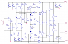
Schematic update:
Attachments
Q16 (not Q9) takes the higher current and should dissipate more power. Q9 passes just 0.6mA (600mV/1k0) and will dissipate just 1mW to 2mW.
AndrewT said:Q16 (not Q9) takes the higher current and should dissipate more power. Q9 passes just 0.6mA (600mV/1k0) and will dissipate just 1mW to 2mW.
Thanks Andrew,
Q9 mounts to the heatsink for thermal tracking. I will use an MPSA56 for Q16.
I'm working to fit everything into the last board layout. This is just a bit easier than creating a brand new layout. 3 new diodes and an extra transistor doesn't sound like a big deal until you need to fit them into an already tight layout.
I haven't tried the 2 transistor bias yet. I didn't feel confident doing it on the working amp - just too many things would need to be changed that could effect the stability, thereby ruining my assessment of the change. I think it's better that I go ahead and make a new board that includes all of the proven changes (feed for bootstrap moved, clamps) and has the second transistor for the bias generator. If it proves to be unusable, I'll simply remove it from the board and change the values of R10.
I need to order the BAV21's from B&D, but I got to thinking: Available only in surface mount at Digikey - am I ready for SMT? I like the idea - not as many holes to drill, even tighter board layout, better availability of (many) parts, cheaper(?).
I'm starting to sway...🙂
Good work ,MJL. All you need now is ambient compensation.
(artic to tropics) i.e. Self's book,page 360. You will have a
real precision Vbias circuit. Am waiting to see your "real world"
findings.
BTW, here's the "poor mans" version heatsink I'll use for
my amp.

OS 😀
(artic to tropics) i.e. Self's book,page 360. You will have a
real precision Vbias circuit. Am waiting to see your "real world"
findings.
BTW, here's the "poor mans" version heatsink I'll use for
my amp.
OS 😀
Ah, the old surplus P3 / P4 coolers. I have a few of those myself. 🙂 Does the job.
I think the 2 transistor bias is going overboard, so I'll stop there. No need for any better bias control.
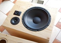
You know, I'm listening to the amp right now. Still no Zobel and running beautifully. The power is has at it's disposal is what separates this from other amps I think.
The speaker it's driving is my older transmission line 2-way with a Vifa PL18 midwoofer and Scanspeak D2905/9500 tweeter. A good speaker and not really a difficult load.
This combo is easily keeping pace with the unit pictured below that I'm using for the left channel - an active 3-way with each driver running off its own LM3886. I built a pair of these for my workshop (yeah, overkill 😀 ).
I think the 2 transistor bias is going overboard, so I'll stop there. No need for any better bias control.
You know, I'm listening to the amp right now. Still no Zobel and running beautifully. The power is has at it's disposal is what separates this from other amps I think.
The speaker it's driving is my older transmission line 2-way with a Vifa PL18 midwoofer and Scanspeak D2905/9500 tweeter. A good speaker and not really a difficult load.
This combo is easily keeping pace with the unit pictured below that I'm using for the left channel - an active 3-way with each driver running off its own LM3886. I built a pair of these for my workshop (yeah, overkill 😀 ).
Attachments
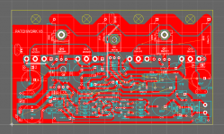
And done. I managed to squeeze it all in and it doesn't look bad. I just need to check it over to make sure I haven't made any mistakes.
My new blank PB boards came, so I'll be able to make this one today. Hopefully all goes well.

My new blank PB boards came, so I'll be able to make this one today. Hopefully all goes well.
megajocke said:Looks nice 🙂
What software is that?
Thanks Mega,
Ultiboard. I see red on black everytime I close my eyes...🙂
What are your thoughts on the 2 transistor bias?
I'm populating the new board now. These new boards are a bit different - the unclad side feels a bit waxy. My silkscreen didn't stick as well. Next time I'll sand it a bit to give it a better grip.
A bit of a pain that I don't have all of the components I need. BAV21 and 47pF silver mica plus I have just ran out of 3.2k resistors.
I'll be giving this one a try later. To be honest, I'm not expecting any surprises.
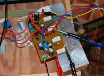
All went well - it's running stable. I have the 100pF Miller cap in place and I'm using the higher pF clamp diodes, so I'll get a better picture on final stability when I get the new parts.
I had to decrease R8 in the Vbe multiplier from 1k down to 470R in order to adjust the idle current. Also, it's very touchy - lucky I have a multiturn pot or it would be very difficult to get the bias dead-on.
I haven't ran it on full supply voltage yet.
The isolation pad right now is a sheet of printer paper smeared with compound. I don't have enough mica left either. I bought a few sheets of thin Kapton film that I was going to cut up and use for pads but I can't punch clean holes through the stuff. 2 pairs of hole punches, one new, both too dull to cut.
Attachments
"The isolation pad right now is a sheet of printer paper smeared with compound. "
Real McGyver style 😀
About the two transistor Vbe multiplier, I'd say it's a more elegant way than the collector resistor to keep bias voltage constant. But both works and with the collector resistor you could make it so that bias voltage decreases with increasing rail voltage if needed.
Real McGyver style 😀
About the two transistor Vbe multiplier, I'd say it's a more elegant way than the collector resistor to keep bias voltage constant. But both works and with the collector resistor you could make it so that bias voltage decreases with increasing rail voltage if needed.
megajocke said:"The isolation pad right now is a sheet of printer paper smeared with compound. "
Real McGyver style 😀
Sometimes you need to improvise. 🙂
I'm not feeling the love for this new Vbe arrangement. It drifts like crazy and I can't seem to do anything to fix it.
Starting off cold, I adjust for ~15mV (55mA) across each of the output emitter resistors. Sitting at idle, it drifts up 3-4mV as the sink warms up. Cut that back to 15mV and give it some signal. It's pulling .5A into the 8ohm dummy load for 20-30 minutes. The load is quite warm and the heatsink is warm also. Cut the signal and measure the idle current again. It's now standing at ~80mV (296mA)!
Now maybe I did something wrong? Were there considerations to take into account for the second transistor? Gain?
In the meantime, the previous board is still operating and playing music. It's been this way for three days. I check the idle current on this one and it's still steady at 55mA.
I think I will abandon this and go back to the single device Vbe, adding the small value collector resistor.
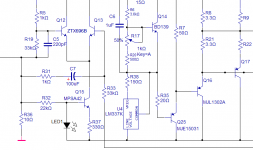
Playing around with another design, I tried something different. I used an LM337 as the current source for the VAS and it seems to perform very well. The sim says it does a better job of restricting output stage current fluctuations when the supply voltage drops or increases.
Will this work properly in this configuration? Or have I got it wrong here.
Will this work properly in this configuration? Or have I got it wrong here.
Attachments
- Status
- Not open for further replies.
- Home
- Amplifiers
- Solid State
- Patchwork Reloaded: Circuit Optimization and Board Layout.