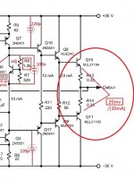
Can Q10e and Q11e voltages be reduced any further.
your heatsink gets so hot because your output power transistors bias current is so high.
Yes, set around this voltages :
Q10e. 10mv
Q11e. -10mv
Your amp is ok to work.
Last edited:
oldjack- have you changed your design from the "page 65" design to BC-1 now?
As patrick showed the "page 65" circuit, I simulated it with no problems, except for high crossover distortion at 20kHz with output transistor bias at 100mA.
Looking at your layout in an earlier post there are a lot of green wires running parallel to each other, which may well have parasitic capacitance.
I would not have expected problems normally, as a 470 ohm degeneration resistor in the input and 30pF capacitor sets the unity gain at 10MHz and that is a stable Miller configuration.
However, with the output triple they are sensitive to stray signals, so I suspect your layout had something to do with your oscillation.
Regarding patrick's advice, and seeing the unexpectedly high crossover distortion, I think a capacitor across the bias transistor is important, along with capacitors across the base-to-base resistors of perhaps 100nF each.
I suspect that the models I have used for the driver transistors (MJE243/253) are not good as I have not checked them and many devices models "out there" are a bit rubbish.
John, no I haven't changed my design to bc1, it won't fit in the space I have but hopefully when I can sort this one out I will modify the circuit layout.
The PCB layout was a trial for a replacement base amp for my existing triamp which is still working but the driver chip is obsolete.
A lot of the jumper wires (those that run parallel with each other) are connections to star gnd.
I have two main star gnd connections, one for clean and one for dirty (power supplies).
I found this stopped any hum on my triamp.
With the bias problems I am finding that reducing R8 makes the bias currents uneven at the power transistors, when I set R8 to give equal bias the voltage measured at the output transistor emitter s is around +/-50mv which pulls too much current through them.
Shoul R7 be higher in value to limit the bias current into Q5.
As patrick showed, you need the currents in the output transistors to be the same. If you are measuring the voltages across the emitter resistors without too much trouble, also measure the quiescent output rail voltage. That should be zero or close to it, or that will cause your output currents to be out of balance.
The feedback resistor does not have to be 19k IMHO - that is Bob just setting the gain to 20 rather than 21. Most of us have a volume control we can use. The input resistor as Patricak also showed should be the same. They could be 22k or if you want a gain closer to 20, 20k. The input should also have a coupling capacitor to prevent offset voltages, and the "grounding" resistor in the feedback line connected through a capacitor too. That will largely equalise the output rail to zero. I'd use 1mF feedback decoupling rather than 220uF - as Doug Self pointed out that reduces distortion. And a 10 or 22uF input capacitor.
Testing these circuits under no load conditions is asking for trouble as the open loop gain is a function of the load, so an open load sends the OLG skywards. Use a 10 ohm-100nF RC pair (output to ground) on the output to prevent disconnected LS sending the gain upwards.
For similar reasons I'd also recommend a 100pF input capacitor (to ground) to keep the input impedance low at high frequencies, since that too can lead to oscillations through HF pickup.
I think Patrick suggested these but there're the main points I'd check before altering the feedback capacitor configuration.
Though the suggestions Patrick made can reduce crossover distortion markedly- from 0.4% to 0.003% if done cautiously, but that can wait until you have your main problem sorted.
Regarding the bias, once you have made the amplifier AC coupled rather than DC, I'd replace R7 (I think - can't check or diyaudio will lose this reply for me) with a 470 ohm and 1k pot and R8 with a2.2k or possibly 2.7k - shold not need to be more than 5x R7 . Triples are more sensitive to this bias, and I'd actually swap the whole circuit for my proposed dual transistor design which can give an exact 6xVbe compensation. For another time perhaps. IF the output rail is zero you should find setting the quiescent current is straightforward, if not a little sensitive to setting.
Last edited:
Regarding the bias, once you have made the amplifier AC coupled rather than DC, I'd replace R7 (I think - can't check or diyaudio will lose this reply for me) with a 470 ohm and 1k pot and R8 with a2.2k or possibly 2.7k - shold not need to be more than 5x R7 . Triples are more sensitive to this bias, and I'd actually swap the whole circuit for my proposed dual transistor design which can give an exact 6xVbe compensation. For another time perhaps. IF the output rail is zero you should find setting the quiescent current is straightforward, if not a little sensitive to setting.
Hi, John
You explained very detail with very good suggestions.
Best regards,
Patrick
Have fitted variable r7 as well as fixed r7.
Measured output rail with no input and read -45mv. This is with 8r resistive load.
The lowest voltage levels I can get on output transistors are (if you subtract offset) +/-50mv
However because of offset this gives actual -100mv/0mv and if I leave it like this the heatsink gets very hot very quickly so I have set it q10 -50mv, q11 -50mv. There is 100mv total.
Is there any way of reducing the offset with no input.
I measured the voltage at the feedback line which is 1.8mv at base of q2.
So I guess this is being amplified to produce the offset.
I am no expert with setting up amplifiers as I was a mechanical engineer but when I built the amp by rod Elliot I did not have any problems setting it up.
This one seems a lot of trouble but I am gradually learning with the help of this forum
I also have found the adjustment of R7/R8 is critical, a half turn too much and the quiescent current through the output transistors rockets.
Maybe your input transistors are not good matched therefore there is -45mv in the output rail.
But for the bias setting, -45mv in the output rail doesn't matter, you just measure both emitter resistor voltage to have a 20mv voltage, each output transistor will have the correct bias current set.
But for the bias setting, -45mv in the output rail doesn't matter, you just measure both emitter resistor voltage to have a 20mv voltage, each output transistor will have the correct bias current set.
Attachments
Last edited:
Whatever adjustments I make for the bias I am unable to reduce the voltage readings at the output transistors to less than 50mv. Are there any other adjustments I can make to lower the quiescent current.
The sine wave is good with my settings but it would be better if I could reduce the quiescent current.
The sine wave is good with my settings but it would be better if I could reduce the quiescent current.
To get the correct bias voltage, you can calculate R7 and R8 as below
Bias voltage(you need around 3.1v) = 0.6 + (0.6/R7)*R8
(all resistor values in ohm)
Bias voltage(you need around 3.1v) = 0.6 + (0.6/R7)*R8
(all resistor values in ohm)
Have you managed to add an input capacitor and a feedback decoupling capacitor?
If you also have equal feedback and input resistors (input base resistor to ground = feedback resistor) then the circuit should not have an offset as large as 50mV I think, but that could well be likely if you still have DC coupling in the feedback loop.
If there is an offset voltage in the output under no load conditions, connecting a loudspeaker will always see an output current, whcih will be Voffset / Rl. That should however be fairly small (your loudspeaker DC resistance might be less than the nominal impedance though).
I do not think that 30mA is necessarily a correct bias. I have only once seen this current as optimum, and that was in the Quad 303 circuit. For complementary output stages I have typically used 50mA, and in a very early design Dr Bailey published, he recommended something in the range 80-120mA (which did include an offset of 20mA though).
What I am a little concerned about is if 100mA is causing your heatsinks to get hot maybe they are not large enough. If, that is, oscillation has now stopped. Otherwise, oscillations might still be causing this.
That is why I advise changing the input and feedback to AC coupling, to minimise DC offsets. You may, as Patrick implied, want also to check that you have matched transistors while you are investigating. If you have a few 2N5401's maybe pick a couple that are matched and use those.
Also, if you add a 10 ohm-100nF RC output load you should be able to measure the quiescent currents without the loudspeaker connected, which should eliminate any offset.
Have done a few more readings and adjustments.
Patrick's formula gives basic ratio as R8=4.16R7
I was quite close to this already but what confused me was the offset of -50mv.
This needed readings of -60mv at q11e and -40mv at q10e to equate to -10mv at q11e and +10mv at q10e. This is very close to what I have.
I set these readings to start with and let the amp soak for about 30min, then reset the resistors slightly. I then ran a 15khz sine wave at input and left it for about 15min.
The output was a clean sine wave at +/-15v.
Heatsink did get quite hot but ok to keep my hand on it.
I already have a 10r/100cap to the at the output.
I also have 220uf cap between R2 and the on feedback line.
I will now redesign the pcb.
But should the heatsinks be increased in size? The previous amp for bass in my triamp has the same size heatsinks with a similar power rating and I have run it ok for 2 years.
What is AC coupling on the feedback line if this is what you recommend.
With my redesign I will try and remove as many jumper leads as possible but the earth leads may have to stay as they all run separately to the two star ground points.
I think the two main problems now are the DC offset and the heatsinks.
I was quite close to this already but what confused me was the offset of -50mv.
This needed readings of -60mv at q11e and -40mv at q10e to equate to -10mv at q11e and +10mv at q10e. This is very close to what I have.
The output offset voltage and the BIAS setting voltage have no relationship with each other, they are independent to each other.
Now you forget and leave the output offset voltage alone.
To do the correct BIAS setting remember below steps :
"You should not measure the voltages Q10e and Q11e to the ground(or to the output)."
You "just measure the voltage between the Q10e and Q11e (emitter to emitter) to get a voltage of 20mv" and then the power transistors BIAS is correctly set.
You use the R7/R8 calculation to set the 20mv on the Q10e and Q11e.
Last edited:
Perhaps I should have said "decoupling" on the feedback line. Your 220uF does that. A capacitor on the input would provide AC coupling. If you still have direct coupling (no cap) that might explain the offset. Just include a 10 or 22uF capacitor in series with the input (and any series resistor present).
Your heatsinks may be adequate. If you are running at +/-35V you should be able to get around 50-60W output (rms). Peak dissipation in the transistors occurs when the output voltage is 2/pi times the supply line, for a sinewave, which for 8 ohm load makes it around 30W for 35V rails and an 8 ohm load.
A 1C/W heatsink will therefore heat up by 30 degrees (this is both transistors on one heatsink), but the transistors will get hotter depending on their thermal resistance and mounting.
At 20 C room temperature that is acceptable (just) but any hotter would need something around the heatsinks for safety. You might get away with a smaller heatsink but it could get very hot.
I usually err on the side of caution, and rather than using sinewaves I calculate the peak dissipation assuming a half power square wave, which in this case would increase the dissipation to 40W. Alternatively you could base the dissipation on a 5 ohm load which could be what an 8 ohm speaker actually is - at some frequency or range.
John, the input base resistor to gnd is 22k but the feedback resistor is only 19k.
You say that these should have the same value, is that correct?
If so I can change the input base resistor as I understand the feedback resistor should be 19k.
You say that these should have the same value, is that correct?
If so I can change the input base resistor as I understand the feedback resistor should be 19k.
You only need the feedback resistor to be 19k if you want the amplifier gain to be exactly 20. If the exact gain value does not matter to you very much then you can use a 22k resistor in the feedback line. The gain is calculated from (Rf+Rg)/Rg where Rf is the feedback and Rg the resistor to ground, so you'd end up with a gain of 23 instead of 20.
I'd probably use 20k myself and have a gain of 21.
However if you also have a resistor in series with the input that will attenuate the input signal, so the gain will be the attenuated input multiplied by the feedback factor.
What is important is that the input and feedback resistors to the bases are the same to minimise the offset voltage. And matching of the two input devices.
I agree with an earlier comment that the circuit you have picked up was probably used as an illustrative "concept" rather than an actual practical one, but it can be made to work as we have indicated.
Last edited:
Ok Patrick, I understand what you are saying about measuring the voltage between Q10e and Q11e.
I will do some more adjustments.
I will do some more adjustments.
Have set the voltage between Q10e and Q11e to 20mv with R8/R7 ratio as you recommend. Yes heatsink ok.
Also when input sine wave signal the output is good and the heatsink ok.
However I have found that I left the signal generator connected to the amp input even when switched off, when I disconnected it the voltage at the amp input was +112mv and the voltage at the output was +65mv
Also when input sine wave signal the output is good and the heatsink ok.
However I have found that I left the signal generator connected to the amp input even when switched off, when I disconnected it the voltage at the amp input was +112mv and the voltage at the output was +65mv
However I have found that I left the signal generator connected to the amp input even when switched off, when I disconnected it the voltage at the amp input was +112mv and the voltage at the output was +65mv
You mean these voltages measured without any input connected
Last edited:
- Home
- Amplifiers
- Solid State
- Parasitic Oscillation