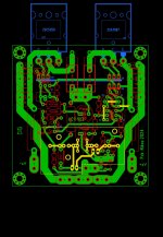
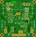
Final version. Option Q7 +Q10+Q8 at the same heatsink.
If someone want the .lay file its free just send me a PM.
If someone want the .lay file its free just send me a PM.
Attachments

Last edited:
Do you really need: fuse sockets + upper mounting holes? Without them you got much more possibilities in routing traces.Nikos
100nF caps - now in your pcb they are 'decoupling' upper legs of fuse sockets (!) ... they should rather be placed close to power transistor legs.

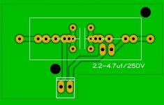
While I agree in concept, this is not the way its implemented on the Wolverine PCB. They have the 100nF caps positioned as Nikos does. Those guys obsessed over every possible PCB tweak that could improve performance. Difference circuit obviously, but the intent of these caps seems the same.
Thoughts?
Thoughts?
I like that layout nikos, and I would like the gerbers to build it please.
Hi my friendI like that layout nikos, and I would like the gerbers to build it please.
You refer about post 67?
Tomorrow when i go to my office i will send it the gerbers.
Can I get the PCB PDF for home etching, if forum rules permits.I must to warning these pcb are untested and unchecked .(post 67)
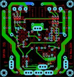

Hello Nikos, have you sent this lay-out to a pcb house? A few thoughts, input source should be away from power sources, yours is very close to rail fuse. another preference of mine is 'rail fuses is placed as part of the PSU board'. One acceptable consideration is 'placing the rail fuses in between a stereo board, just like Rod Elliotts pcb design.Final definitions.....personal use.
This is my personal preference of a CFP output amp board. Outputs, drivers and zobel network is placed near each other, the more compact the better.
Attachments

By the way, you may want to delete or edit ESP P3A on your board. Your board is a moded version and does not follow the original scheme of ESP. 😉
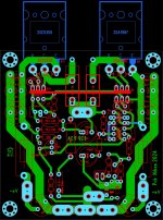
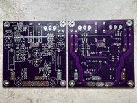
I gave a Nikos' boards a run.
Just the pcb, no soldering so far.
Silk screen is as you can see on the picture.
Misleading 2SA1943 marks are left near OPS transistors.
The main issue is with drilling - too small holes for many components.
Resistors with 0.55mm leads does not fit.
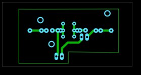
Example - 10R/2W resistor on one lead is D12, on the second is D13 (on the drill map).
In my opinion D11 should not be used, all D12 should be reviewed.
I got a few spare boards (say 4 pairs to share).
If someone wants to give it a try (boards as is, manual correction of drilling is needed) please PM me.
Across EU shipping is like 7 EUR, boards 3 Eur per pair, total 10Euro.
Just the pcb, no soldering so far.
Silk screen is as you can see on the picture.
Misleading 2SA1943 marks are left near OPS transistors.
The main issue is with drilling - too small holes for many components.
Resistors with 0.55mm leads does not fit.
Example - 10R/2W resistor on one lead is D12, on the second is D13 (on the drill map).
In my opinion D11 should not be used, all D12 should be reviewed.
I got a few spare boards (say 4 pairs to share).
If someone wants to give it a try (boards as is, manual correction of drilling is needed) please PM me.
Across EU shipping is like 7 EUR, boards 3 Eur per pair, total 10Euro.
Attachments
- Home
- Amplifiers
- Solid State
- P3A PCB Layout