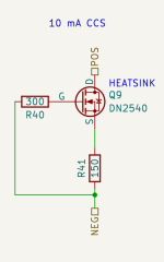
Standard deviation of FETs parameters (mainly IDSS) will be enough large. Matching (or rather measuring) its for IDSS filters out weaker ones (generally similar IDSS gives similar gfs too) .... and fakes too.
Once I bought -cheap- 100 pcs J310 and measure its. All of them was fake, probably relabelled (below 10mA) K170.
If the gyrator output impedance is important, the lower FET forward transconductance (gfs) is defining parameter.
Approximate data:
J310 (with enough large deviation) 13mS (8-18mA depending of manufacturer);
J113 0.5-30mS;
2SK170 22mS;
BF 862 45mS;
AOT1N60 900mS.
Each of them datasheet shows "from-to" or defined gfs data, but all measured at ten-few ten D-S voltage.
The method of use -in this case- gives -about- 1-2V, so gfs degrading here, but generally higher datasheet value gives lower output impedance.
So AOT1N60 theoretically is better here than J310 .... but a little unpractical.
The first is TO220, the second is TO92 cased, AOT1N60 has -even- 1A capability, the matched/measured J310 is appropriate for 20-30mA application.
If the gyrator output impedance is important, the lower FET forward transconductance (gfs) is defining parameter.
Approximate data:
J310 (with enough large deviation) 13mS (8-18mA depending of manufacturer);
J113 0.5-30mS;
2SK170 22mS;
BF 862 45mS;
AOT1N60 900mS.
...
So AOT1N60 theoretically is better here than J310 .... but a little unpractical.
...
The 2SK170 is limited to less than 20 mA, the BF862 is SMD only. The J310 and J113 would work ok. However, the AOT1N60 has much higher gfs, and I don't see anything unpractical about it. I guess we can stick to the AOT1N60.
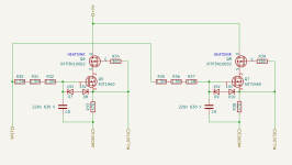
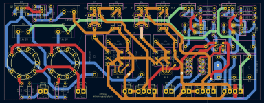
Here's one more iteration of the amp schematics and also a first attempt of a PCB layout. I am a total noob with PCB design and KiCad!
The amp schematics show the changes related to the recent discussions. The main change is the added filter caps on the amp boards, and the removal of some Zeners. I also realised that the HOT/COLD signal polarity got upside down after the buffer FETs, so I also fixed this.
The amp schematics show the changes related to the recent discussions. The main change is the added filter caps on the amp boards, and the removal of some Zeners. I also realised that the HOT/COLD signal polarity got upside down after the buffer FETs, so I also fixed this.
Attachments

1.27k x 4 for the output resistor. To increase the probability that at least one will open if necessary?
Mounted vertically, do they reduce space and allow for an easy test point?
I like it more and more.
Mounted vertically, do they reduce space and allow for an easy test point?
I like it more and more.
That's the idea. My hypothesis is that going from a 2W resistor to a 0.5W resistor, the mass decreases by by more than the ratio of the power rating (i.e., by more than a factor 4). This would mean they heat up quicker, so they would fail quicker. That will need testing.1.27k x 4 for the output resistor. To increase the probability that at least one will open if necessary?
Less space and less cooling if things go wrong. I didn't think of the test point idea, but that makes sense, too!Mounted vertically, do they reduce space and allow for an easy test point?
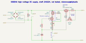
After discussion with @PretentiousFood over in the Power Supplies forum, I changed the HV PSU draft as follows (see attachment):
- Changed the output FET to NTHL1000N170M1
- Removed the buffer coupling the voltage reference to the gate of the output FET
Attachments
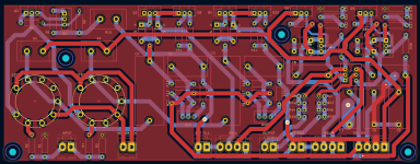
Here's a draft of the PCB for the power supply of the high voltages and heaters for the input stage (the raw DC for the DHT Coleman regulators will be on a separate board).
What do you guys think?

What do you guys think?
The spacing seems to be a little close in the critical area.
The first pic is my failed attempt at a HV board for the Quad ESL57: arc at the upper left hand side:

V1.21, the second attempt works:

Of course, these boards deal with 6KV, so YMMV.
The first pic is my failed attempt at a HV board for the Quad ESL57: arc at the upper left hand side:
V1.21, the second attempt works:
Of course, these boards deal with 6KV, so YMMV.
Ah, oh, aehm. I didn't think of arcing at all... and I don't know much about it.
With the estat bias of +580 VDC and the grid bias / buffer supply of -550 VDC, the max. voltage between tracks would be 1130 VDC on the amplifier board. On the PSU board it might be slightly more right after the rectifiers, but not much.
What is the typical/recommended limit for the distance between tracks for a given voltage? Does that scale linearly with voltage?
The working board in your example uses both the top/bottom layers. The distance between the tracks is only the thickness of the board. Will the board material prevent/reduce arcing?
Me neither, that's the feeble excuse for the 1st fail. 🙂
Rule of thumb: air is terrible, anything else buys you at least 10x improvement. Experimental proof: the arcs I observed were between the exposed wires of the parts. Also, the V1.21, while safe by itself, arced merrily between the board and the mounting; easily fixed by placing an old credit card in between; the card was subsequently replaced by a piece of plastic, for looks alone.


Rule of thumb: air is terrible, anything else buys you at least 10x improvement. Experimental proof: the arcs I observed were between the exposed wires of the parts. Also, the V1.21, while safe by itself, arced merrily between the board and the mounting; easily fixed by placing an old credit card in between; the card was subsequently replaced by a piece of plastic, for looks alone.
The breakdown voltage in air is something in the range of 1-3 kV/mm (see https://electronics.stackexchange.com/a/544603 ).
I guess it would be a good idea to keep the trace distances at >1 mm/kV or so. I'll check the boards and adjust where necessary.
Thanks for bringing that up!
I guess it would be a good idea to keep the trace distances at >1 mm/kV or so. I'll check the boards and adjust where necessary.
Thanks for bringing that up!

Freon has been legislated-away, by congress, so it is no longer available.
It was used to clean the rosin off of PCBs (between traces and between pads)
Alcohol works, but takes more work, and multiple applications to be effective.
Rosin causes Arcs, the issue is not only the minimum air distance for Arcing.
'Nuf Said
It was used to clean the rosin off of PCBs (between traces and between pads)
Alcohol works, but takes more work, and multiple applications to be effective.
Rosin causes Arcs, the issue is not only the minimum air distance for Arcing.
'Nuf Said
Clearance and creepage are the relevant terms. Clearance is for air, creepage is for surface conduction (which is very humidity dependent). Any gap less than about 7mm can be bridged by a curious ant too, another factor to consider in some situations!
Milled slots in PCBs are one technique for handling creepage.
Milled slots in PCBs are one technique for handling creepage.
You may already be aware, but there is some very upsetting precedent involving ants and Stax.Any gap less than about 7mm can be bridged by a curious ant too, another factor to consider in some situations!
https://www.head-fi.org/threads/ants-in-my-stax-should-i-worry.609792/
KiCad does offer some tools for calculating creepage, sort of. Ants aside, 2-3mm sounds right. If nothing else, this helps keep stray capacitances down in a design where slew rate is critical. 🙂
Hmmm. Is it possible to apply these rules to automatically check a PCB in KiCad?KiCad does offer some tools for calculating creepage, sort of.
You can set required spacings in KiCad and I think you can make them dependent on net classes (or whatever the term was). The DRC will then warn you when the spacing is insufficient. Getting each net into the right class is still manual work.
Hmm, yes, I could specify different spacing values for the different nets / netclasses. However, that would mean KiCad would apply the same spacing everywhere along these traces. However, we'd want 2-2.5 mm between B+ and B- traces only (and similar for B+ and neg. bias), but could live with about half this clearance between B+ and GND or between B- and GND.
I guess it's a bit of work anyway, so we could just set a minimal "overall" clearance, and then check manually for some extra clearance between the traces carrying the more extreme voltages.
If someone has more ideas and wants to play with the files, they are here: https://github.com/mbrennwa/OSDEHA
Here's what I did as a temporary amplifier board version (won't use that for the final production):check manually for some extra clearance between the traces carrying the more extreme voltages.
- Changed board to 4 layers
- Moved all traces that are at > 400 V to a separate layer (green)
- Moved all traces that are at < 400 V to a separate layer (yellow)
- Checked for separation between green and yellow traces (by eye)
Attachments
You can define custom DRC rules to do this type of stuff. Go to Board Setup > Design Rules > Custom Rules and click the Syntax Help link.
Some examples:
Some examples:
(rule "copper keepout"
   (constraint disallow track via zone)
   (condition "A.intersectsArea('zone3')"))

(rule "BGA neckdown"
   (constraint track_width (min 0.2mm) (opt 0.25mm))
   (constraint clearance (min 0.05mm) (opt 0.08mm))
   (condition "A.intersectsCourtyard('U3')"))

# prevent silk over tented vias
(rule silk_over_via
   (constraint silk_clearance (min 0.2mm))
   (condition "A.Type == '*Text' && B.Type == 'Via'"))

(rule "Distance between Vias of Different Nets"
    (constraint hole_to_hole (min 0.254mm))
    (condition "A.Type == 'Via' && B.Type == 'Via' && A.Net != B.Net"))

(rule "Clearance between Pads of Different Nets"
    (constraint clearance (min 3.0mm))
    (condition "A.Type == 'Pad' && B.Type == 'Pad' && A.Net != B.Net"))

(rule "Via Hole to Track Clearance"
    (constraint hole_clearance (min 0.254mm))
    (condition "A.Type == 'Via' && B.Type == 'Track'"))

(rule "Pad to Track Clearance"
    (constraint clearance (min 0.2mm))
    (condition "A.Type == 'Pad' && B.Type == 'Track'"))

(rule "clearance-to-1mm-cutout"
    (constraint edge_clearance (min 0.8mm))
    (condition "A.Layer == 'Edge.Cuts' && A.Line_Width == 1.0mm"))

(rule "Max Drill Hole Size Mechanical"
    (constraint hole_size (max 6.3mm))
    (condition "A.Pad_Type == 'NPTH, mechanical'"))

(rule "Max Drill Hole Size PTH"
    (constraint hole_size (max 6.35mm))
    (condition "A.Pad_Type == 'Through-hole'"))

# Specify an optimal gap for a particular diff-pair
(rule "dp clock gap"
    (constraint diff_pair_gap (opt "0.8mm"))
    (condition "A.inDiffPair('/CLK')"))

# Specify a larger clearance around any diff-pair
(rule "dp clearance"
    (constraint clearance (min "1.5mm"))
    (condition "A.inDiffPair('*') && !AB.isCoupledDiffPair()"))

# Don't use thermal reliefs on heatsink pads
(rule heat_sink_pad
    (constraint zone_connection solid)
    (condition "A.Fabrication_Property == 'Heatsink pad'"))

# Require all four thermal relief spokes to connect to parent zone
(rule fully_spoked_pads
    (constraint min_resolved_spokes 4))

# Set thermal relief gap & spoke width for all zones
(rule defined_relief
    (constraint thermal_relief_gap (min 10mil))
    (constraint thermal_spoke_width (min 12mil)))

# Override thermal relief gap & spoke width for GND and PWR zones
(rule defined_relief_pwr
    (constraint thermal_relief_gap (min 10mil))
    (constraint thermal_spoke_width (min 12mil))
    (condition "A.Name == 'zone_GND' || A.Name == 'zone_PWR'"))

# Prevent solder wicking from SMD pads
(rule holes_in_pads
    (constraint physical_hole_clearance (min 0.2mm))
    (condition "B.Pad_Type == 'SMD'"))

# Disallow solder mask margin overrides
(rule "disallow solder mask margin overrides"
    (constraint assertion "A.Soldermask_Margin_Override == 0mm")
    (condition "A.Type == 'Pad'"))

# Enforce a mechanical clearance between components and board edge
(rule front_mechanical_board_edge_clearance
    (layer "F.Courtyard")
    (constraint physical_clearance (min 3mm))
    (condition "B.Layer == 'Edge.Cuts'"))

# Check current-carrying capacity
(rule high-current
    (constraint track_width (min 1.0mm))
    (constraint connection_width (min 0.8mm))
    (condition "A.NetClass == 'Power'"))

# Separate drill bit and milling cutter size constraints
(rule "Plated through-hole size"
    (constraint hole_size (min 0.2mm) (max 6.35mm))
    (condition "A.isPlated() && A.Hole_Size_X == A.Hole_Size_Y"))

(rule "Plated slot size"
    (constraint hole_size (min 0.5mm))
    (condition "A.isPlated() && A.Hole_Size_X != A.Hole_Size_Y"))
- Home
- Amplifiers
- Headphone Systems
- Open Source DHT Estat Headphone Amp -- OSDEHA