...never had a MV ion implanter with enough beam current to get the oxide layer deep enough.
Would have thought higher beam energy would be the way to go deeper?
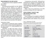
Yes, but how many MeV would be needed to go deeper? For medical purposes, beam energies from about 50KeV up to around 250MeV may be found. What about for ion implantation in semiconductors?
https://www.renesas.com/in/en/www/doc/datasheet/hfa3046-3096-3127-3128.pdf
Some of the few fast-ish PNPs still alive.
IIRC, the whole family is just bond-out options of a 4*4 transistor array.
Somewhere I have a chip photo.
Gerhard
Some of the few fast-ish PNPs still alive.
IIRC, the whole family is just bond-out options of a 4*4 transistor array.
Somewhere I have a chip photo.
Gerhard
Can't imagine anything over 4-5" silicon on sapphire wafers, but I may be rusty since I worked in a fab (2" at the time, don't ask the cost 😀)
Sorry, I was referring to TI having a 200mm isolated process, tops. Maybe still 150mm. Pretty sure SoS is 100mm. I never did SOI, but did wafer bonding for a specialized process to create an extremely deep PIN diode structure (the undoped layer being on the order of 150um thick, so that was a case of bonding a highly doped wafer to an undoped (extremely lightly doped) wafer, and then lapping back, implanting, annealing, lapping surface.
Global Foundries has a few different SOI technologies, some with very thin Box (Buried oxide layer). They have been promoting the 22nm FD-SOI (Fully Depleted Silicon on Insulator) for quite awhile.
One of my engineering instructors once referred to Silicon On Sapphire as $O$.
Another company using SOI - pSemi - Intelligent Electronics for the Connected World
He was involved with the "gate first" SoC-on-SOI process at GF, which I think is at 12nm now. Anyways, we're a biotech company, so new challenges. 🙂
And I had forgotten to put the link to PSemi when I alluded to a "San Diego SoS company". One of their founders gave a talk at my uni a while ago, but, yes, we're talking the same company. 🙂
Yes, but how many MeV would be needed to go deeper? For medical purposes, beam energies from about 50KeV up to around 250MeV may be found. What about for ion implantation in semiconductors?
Apparently, for implanted Box the energy is only 200keV, but the current is high at up to 100mA.
http://accelconf.web.cern.ch/PAC2013/papers/weyb2.pdf
https://www.hitachi.com/rev/pdf/2002/r2002_03_108.pdf
Attachments
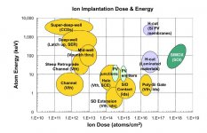
This is for FDSI CMOS (very shallow BOX, voltages of a few volts max). For analog devices, the BOX must be much deeper, since FDSI operation is not possible. Here's a reference for 2.5MeV oxygen implantation https://www.collectionscanada.gc.ca/obj/s4/f2/dsk2/tape15/PQDD_0012/NQ35573.pdf
Last edited:

It is not easy to imagine a 2.5MeV ion implanter, able to deliver 100mA or more of beam current. The power supply needs to be 2.5MV, that's 2,500,000 volts, and a power of at least 500KW. And that power needs to be somehow dissipated/cooled to avoid a general meltdown. Essentially a giant 2 stage water cooled vacuum tube, with 3 stages of vacuum pumps (roughing, turbo, ion getter). Has a ECR (Electron Cyclotron Resonance) ion source. An apocalypse machine, could be used in a Mad Max movie.
P.S. You don't stay anywhere close when the machine is running, if you value your health and life. Bremsstrahlung (cyclotron radiation, in this case) is not funny to ingest.
P.S. You don't stay anywhere close when the machine is running, if you value your health and life. Bremsstrahlung (cyclotron radiation, in this case) is not funny to ingest.
Last edited:
Sorry, deleted post. Will think more about it overnight. But yes, water cooled tubes, 8' thick borated concrete walls around the cyclotron room (for neutron capture), etc. Don't know if these machines are ever used for semiconductor ion implantation.
Last edited:
I think the MeV implanters are running lower currents than for the shallow SOI implant.
For higher voltage (> 10V) SOI, the bonded wafer approach is probably much more practical.
For higher voltage (> 10V) SOI, the bonded wafer approach is probably much more practical.
Last edited:
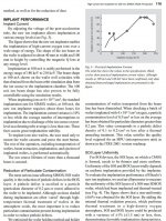
Depends. There is a range of silicon thicknesses that make the SIMOX process impractical. It is very difficult to polish to a, say, 10um thickness without cracks and induced stacking faults in the silicon, that cannot eventually be gettered also due to the limited thickness.
I am pretty sure the BB SOI process for Difet is a version of SIMOX (wafer bonded) process. I don't think anything else was available in production at that time (other than the crazy SOS), and I vaguely remember seeing some patents about.
Enough of this, otherwise I'll have nightmares about the phosphine and arsine bottles tonight 😀.
.... Enough of this, otherwise I'll have nightmares about the phosphine and arsine bottles tonight 😀.
Back in the days when the Fab was in the same building as the design lab, there was a microwave in the lab, that people used for heating lunch. It had a sign on it that said no trout almondine allowed in the microwave.
The problem with the old bonded wafer DI process for 36V Analog is the equipment and many of the Fabs are old (replacement equipment parts can be hard to find) & have limited capacity. The Manufacturing side of the company often just raises wafer costs till the Product line drops the process use (or the product line is forced to an outside foundry). In the meantime ,the product price raises to cover the cost of manufacturing. To invest in new Fab equipment for any newer process technology requires a Product line commitment for adequate long term wafer volume with good margins.
It more practical & cost effective to use the newer high volume ICs for new designs (that are run on high volume process technologies). There are many newer Audio quality Op Amps available, that are much more cost effective than the very old BB DI products. There are newer products that are a much better value, even if one chooses not to use the excellent OPA1656, see attached
It more practical & cost effective to use the newer high volume ICs for new designs (that are run on high volume process technologies). There are many newer Audio quality Op Amps available, that are much more cost effective than the very old BB DI products. There are newer products that are a much better value, even if one chooses not to use the excellent OPA1656, see attached
Attachments

I'm using the OPA1612 in a new design, and a phenomenal piece of work that it.
Why, with so many zeros in the distortion figure don't TI quote it in ppm? 0.15ppm is much easier to understand and compare performance figures than 0.000015%
The comparison would be quoting capacitance in uF regardless of size - 4.7pF is easier to understand than 0.0000047uF
Why, with so many zeros in the distortion figure don't TI quote it in ppm? 0.15ppm is much easier to understand and compare performance figures than 0.000015%
The comparison would be quoting capacitance in uF regardless of size - 4.7pF is easier to understand than 0.0000047uF
Last edited:
I agree that the 0.000015% figure is unwieldy. But if you look farther down in the data sheet, it is quoted in db (-136db) which is even easier to deal with than ppm.Why, with so many zeros in the distortion figure don't TI quote it in ppm? 0.15ppm is much easier to understand and compare performance figures than 0.000015%.
I think the MeV implanters are running lower currents than for the shallow SOI implant.
For higher voltage (> 10V) SOI, the bonded wafer approach is probably much more practical.
Another option is to grow oxide on a wafer. Then grow epitaxial silicon on top. Build the devices in the EPI.
I seem to recall that you can buy wafers that already have this work done.
Tom

- Home
- Vendor's Bazaar
- OPA1656: High-Performance CMOS Audio Op Amp