A resistor requires extra positive current from the upper LM317 and clips early on the negative cycle, ie 50% neg Voltage, ~25% max power output. A BJT or MOSFET requires more devices to make a CCS but not really a problem. A JFET with a Idss more than about 100mA are not common. The classic single ended pull-up/down is an inductor which stores current and provides a pseudo ~negative power supply.
Personally, I would at least use a P-P output, even if it was still class-A. Efficiency is much better.
Personally, I would at least use a P-P output, even if it was still class-A. Efficiency is much better.
Hi sorry it is me again Are these your requirements ? i mean do you have to push 5V on a 500ohm load ?I am sorry, do I read correctly H2 at -64dB , In 5V and 500Ohm?
These simulation results are not at the level which I need. The LM317 can do much better at the same load or even stronger ones.
Not really for me (tape has its own physics working as limiter) but a good safe margin is always a necessity. Good machines have in excess of +18dB margin.Hi sorry it is me again Are these your requirements ? i mean do you have to push 5V on a 500ohm load ?
I'd say +13dBV (5V) is a reasonable test (implicit requirement). As a matter of fact I am stress testing the buffer using at least +12dB.
Yes, it was mentioned somewhere in previous pages.
I'd say it is usual to show THD performances on stress tests, as opposed to show THDs only on the nominal 0dB.

I assume that PP means pull-pull and 317 is not one of them (both class A).Personally, I would at least use a P-P output, even if it was still class-A. Efficiency is much better.
Efficiency is not much of concern here. I mean, dissipation up to 1-2W is manageable for any kind of component. Right?
this answer needs my attention and study. This is also a part of what I am here for. Thanks!A resistor requires extra positive current from the upper LM317 and clips early on the negative cycle, ie 50% neg Voltage, ~25% max power output.
this not.The classic single ended pull-up/down is an inductor which stores current and provides a pseudo ~negative power supply.
Choosing capacitance to be the standard for reactive energy reservoir, I would personally never mix-in a coil for the same purpose.
Maybe you are right, but I don't fully understand your point.
is a shorted FET not a "two leads" CCS likewise a large resistor?A BJT or MOSFET requires more devices to make a CCS but not really a problem.
What do you mean 'requires more devices'? An example will help my understanding...
JFETs or (rare) depletion mode MOSFETs can be used as a CCS by shorting the gate and source because the useful gate voltage is below the source voltage, opposite the drain voltage. But typical MOSFETs are enhancement mode and require a gate voltage the same polarity as the drain. If you ~ground the gate of a MOSFET, the result is ~zero current. Depletion mode MOSFETs do exist but they are rare and expensive, as are power JFETs. JFETs make great CCS, but not typically available for currents over 100mA. To make a CCS from a BJT or typical MOSFET, you need a base/gate bias voltage, which requires a few more parts, like in wrenchone's circuit, post #277. One problem with JFET CCS's is that the Idss of a given JFET has a spec that may be a 10:1 range, so a pot or selected source resistor is often used to adjust the current. For a DIYer, selecting JFETs is not a problem, but a deal breaker for mass production.
Fresh in the morning, this reminds me of SMPS and tuned autotransformers. Probably 'classic' in this context, I guess.The classic single ended pull-up/down is an inductor which stores current and provides a pseudo ~negative power supply.
Can you show an example how you think this expertise can be used in a audio buffer?
this seems to be a more general issue, or question.A resistor requires extra positive current from the upper LM317 and clips early on the negative cycle, ie 50% neg Voltage, ~25% max power output.
Can we not choose a stronger regulator version, or change the bias settings?
I built it and the results were slightly better than simulations: using 2xBC550B and for 0dBu the H2 is ca. -104dB. The noise was nice at -107dB (with 4096bins in 20KHz) and H3+ were slightly below this level.With R1=22K load Tina gives this result: see below. It is slightly worse THD (0.003%) than the LM317 optimized by LV and Marcel, but let's see about the noise.
With 10KOhm loaded lines the THD will increase to 0.01% and for Headphones 600Ohms the THD will further increase to 1.8%, according to Tina. Maybe it is not optimized...
In contrast, the LM 317 performance for THD is stable also with strong loads.
Still, I will try to build it to verify and let you know.
View attachment 1313239
One question: I was not successful to find its input impedance Zin by simulations. Do you have an estimate for it?
(seems to be lower than LM317 configured as per LV schematics with 2x20KOhm biasing, could this result be true?)
Could it be that it is less than 1KOhm?
The input impedance is probably greater than 100K, certainly not 1KOne question: I was not successful to find its input impedance Zin by simulations. Do you have an estimate for it?
(seems to be lower than LM317 configured as per LV schematics with 2x20KOhm biasing, could this result be true?)
Could it be that it is less than 1KOhm?
I have another 2xBJT proposal for a buffer, this time inspired by the Revox's TIA ideas (Rec amp stripped by EQ, and of course modify the gain settings resistors): the simulation results are very good or at least decently good (SNR>130dB, THD<0.0002%)... Clearly a better contender for 1xBJT (inclusive also the simple LM317 without CCS) ... BUT only up to 1dBu input!
Headphone requirement is out for this proposal. I can simulate good performance with >2Kohm loads.
Still, somehow I cannot find a solution to avoid the asymmetric clipping at around 1.3V. Or, if I find a way to increase clipping to 2.3V, then distortions are horrible.
Any helping hand please, to bring the clipping at >6V and still keeping the small THD+N?
Attachments
Mostly a basic arithmetics problem: you try to drive a 2K load with a stage having a collector load of 6K8.Any helping hand please, to bring the clipping at >6V and still keeping the small THD+N?
R5 and R4 should be at least 5x smaller.
In addition, the quiescent base voltage of T2 might be somewhat insufficient for the excursion you envision.
Proper DC bias conditions should be established before trying to go further
Thanks, I do believe it is basic arithmetics but I also believe it depends who you ask.
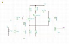
I am staring at this circuit for more than 1 year and I still cannot understand it, nor I find anywhere to read how it works (even less how to compute its bias. All I see is chocking everywhere, up and down. Playing with parameters, I see too many 'windows' and I am already dizzy... a nightmare for me.
Say the least, I am curios to learn what the proper bias is when defined by experts. A few explanatory words from professors will be also helpful.
Then, the THD aspect which is seen to perform 'good' only when bias of second BJT is 'wrong'.
I am staring at this circuit for more than 1 year and I still cannot understand it, nor I find anywhere to read how it works (even less how to compute its bias. All I see is chocking everywhere, up and down. Playing with parameters, I see too many 'windows' and I am already dizzy... a nightmare for me.
Exactly the help asked 🤔Proper DC bias conditions should be established before trying to go further
Say the least, I am curios to learn what the proper bias is when defined by experts. A few explanatory words from professors will be also helpful.
Then, the THD aspect which is seen to perform 'good' only when bias of second BJT is 'wrong'.
single progress which I have done myself, is to see that R3 sets the 'Aol' and the R8 is the 'Rf' (naming conventions of TIA for opamps).
Of course, this is good - but not enough.
Of course, this is good - but not enough.
I know that number of answers is inversely proportional to number of questions, but I am desperate enough to try my chance.
In contrast to above, from below I understand that output is not exclusively T2, but also T1.
The output node always puzzled me: say 15uA into C3, plus 200uA into C4 and 250uA into R6 (all with phase, such as sum is null). This supports the statement above.
Then, the 2K load should necessarily scale the R4 and R5, or the R2 and R3? Apparently the latter.
But then, what is the role of the T2, apart from being instrumental in making a virtual ground in the T1 base?
And, how it is then proper to bias such circuit? In simulations I see that smaller R2 makes things go wild and higher R2 effect is to tame it.
Any case, question is how this circuit is supposed to work "nominally"? The higher the Aol gain (as amplifier) makes T2 contribute more and more to the output node (hence R4, R5 more relevant) and the lower the gain (as buffer) makes T1 contribute more to the output than T2?
To rephrase: if I want to add a CCS, where should I place it and how to compute it?
Correction: for this particular set of parameters actually not.The output node always puzzled me: say 15uA into C3, plus 200uA into C4 and 250uA into R6 (all with phase, such as sum is null). This supports the statement above.
T4 is the main output transistor; T2 is the error amplifier.
In fact, the circuit is conceptually a CFP, but it uses same-sex transistors which complicates the implementation and necessitates various capacitors. The topology could be useful where only N-devices are available, eg. tubes, but with transistors, the best option is to use the regular CFP. The performances can be made identical if the transistors are of a comparable quality.
The logical place to put a CCS would be to replace R4, but it would be problematic since the voltage on the collector of T4 would become undetermined: the sense for the DC feedback is taken from the emitter
- Home
- Source & Line
- Analog Line Level
- One BJT line amp/buffer