The DIYAudioStore has the Linear Systems counterparts (LSK170/LSJ74) in stock right now.
Also, if you drive the amp with a low output impedance (low meaning less than 100 ohms) pre-amplifier, you can bypass the input buffer formed by the two JFETS.
Also, if you drive the amp with a low output impedance (low meaning less than 100 ohms) pre-amplifier, you can bypass the input buffer formed by the two JFETS.
I think I did see that, I went back and looked again though. I don't mind drilling and tapping holes, but I really like this method/hole spacing! It was a lot faster as I just used the PCB as the template, aligned + center punched all the holes, and went to town with my drill press. Plus I could tighten everything down without the risk of stripping out any holes.I don't know if you saw it, but in January of 2016 I posted pictures of standoffs installed using through holes, as you described.
Looking back through the thread I also can't believe it was that long ago that I signed up for your PCBs! Time flies I guess. After the M2 and B1 (95% done) I have a set of F6 boards fully stuffed, just waiting for FETs and heat-sinks. There's a set of F5 boards sitting in one of my drawers somewhere. There's a VFET kit waiting patiently on the corner of my bench. A BA3 front end fully built sitting in another drawer, intended as a line amp if I ended up needing some gain. Not to mention two large(ish) Rubbermaid tubs full of tubes and some bits of Electra-Print iron I've procured throughout the years. So little time, but it's nice to be dipping my feet back into this hobby.
As for my issue regarding the left channel bias. I still need to go through the board tonight and check all the resistor values. However, could a faulty LM385 be playing a roll? I just want to make sure too that I am correct in understanding that R11 (221R resistor) sets the bias. I'm going to try and find time to get this all sorted out by the weekend, I want to give this thing a listen!

Double check the resistor values and, most of all, make sure the opto-couplers are positioned correctly. The notch and dot on the device must match the silk-screen on the PCB.
The opto-couplers appear to be positioned correctly (glad I used sockets on those) and all the resistor values appear to check out. I traced everything on the pcb and it all seems to check out fine, I wanted to ensure that the coupler was in there correctly. Pin #1 is the LED anode, which is marked with a dot on the Vishay 4N35s that I am using. On the left channel PCB, mounted with the FETs pointed down, the pin #1 dot should be in the upper left corner.
If the opto-coupler was in there backwards it wouldn't work at all right? I need to look closer at the back of the board, but is it possible I could have a solder bridge lurking across one of the LM385s?
If the opto-coupler was in there backwards it wouldn't work at all right? I need to look closer at the back of the board, but is it possible I could have a solder bridge lurking across one of the LM385s?
What if?
What if? Number one
I thought about doubling output fets keeping the same bias. IT would be necessary to change 0,47 to 1 ohm, but wwhat about 100 ohms? Add next 100 ohm to Gates od seconda pair of fets?
What if? Number 2
If i will not be Happy with transformer soundtrack, i think IT would be possible to replacement IT with double rail clone od jfetboz? Or opamp with 15 gain?
@ Wrath
M2 is unique amplifier.
Not many have inside autoformer passive gain stage.
That is the heart.
Other front-end with the jfets or op-amps
and you be never know true spirit and sound of this non feedback amplifier.
20 watts is plenty of power with efficient speakers especially with 4 ohm's
you get twice so non need for parallel transistors output stages.
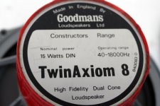
Goodmans Axiom8 is happy with 15 watts for example 😉
M2 is unique amplifier.
Not many have inside autoformer passive gain stage.
That is the heart.
Other front-end with the jfets or op-amps
and you be never know true spirit and sound of this non feedback amplifier.
20 watts is plenty of power with efficient speakers especially with 4 ohm's
you get twice so non need for parallel transistors output stages.
Goodmans Axiom8 is happy with 15 watts for example 😉
Attachments
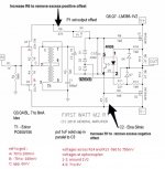
Offset regulation is more easy and precise with add of another trimmer connected to R7.
Maybe future M2 pcb's in DiyAudio Store can be with this option included.🙂Greetings
Maybe future M2 pcb's in DiyAudio Store can be with this option included.🙂Greetings
Attachments

considering that there is already one trimpot in series with R6 ........ really only possible leap in comfort of building that amp is ........... that someone else builds it for ya

He is still enamored with odd-looking components. One of these days he will take the time to learn how circuits work.
In the meantime, I think you made him "SoundSad"...

In the meantime, I think you made him "SoundSad"...
I have do it and work very well for me.considering that there is already one trimpot in series with R6 ........
really only possible leap in comfort of building that amp is ........... that someone else builds it for ya
In a situation of excess negative offset
with the series connected trimmer to R7
that precise resistance value is made easy for optimal ~ 0 MV offset.
Without that you roll resistors in R7 position who are soldered and re soldered on the pcb to find right spot ?
Sorry....ooouhhh
Attachments
Last edited:
Without that you roll resistors in R7 position who are soldered and re soldered on the pcb to find right spot ?
Earlier in this thread Nelson Pass described different aspects of how the circuit works and reminded builders that the commercial version used Fairchild devices.
After I built my own PCBs I talked about adjusting the resistor values when using IRFP240/IRFP9240 MOSFETs. Zen Mod also added information regarding adjusting the offset. As you can see, other people already provided ALL the information you need. You just failed to read it.
🙁
Yeah not build guide for this one.
Read all thread is hard to do.
I do use 10K trimmer ( 2K5 position at start )
so not worry about incrase of resistors if needed.
I provide one more information so that not ALL 😉
He is still enamored with odd-looking components.
One of these days he will take the time to learn how circuits work.
In the meantime, I think you made him "SoundSad"...: sad:
In the meantime, I think don't make you " Grumpy berg "
or be disrespectful and ironical.
For the expert : You need advices?
Find the answer by yourself in + 2000 thread post's.
What is collaborative participation to grow ?
A silly idea:
What about soldering machine pin sockets at R6 and R7 and then
start by fitting them with the nominal 47K resistors? One can
then easily adjust the resistors as required and then add a little solder
from the top after verifying that P1 can null the offset.
What about soldering machine pin sockets at R6 and R7 and then
start by fitting them with the nominal 47K resistors? One can
then easily adjust the resistors as required and then add a little solder
from the top after verifying that P1 can null the offset.
it seems this null offset becomes so complicated, come on guys. ZM advice on on this picture should be easy, you are smarties. even me as a dumbies can implement it easily

it seems this null offset becomes so complicated, come on guys. ZM advice on on this picture should be easy, you are smarties. even me as a dumbies can implement it easily
+1 This isn't hard to do. I had to change the values around because I used 2sk1530/2sj201 for the output devices, and all it takes is a little experimentation.
+1 This isn't hard to do. I had to change the values around because I used 2sk1530/2sj201 for the output devices, and all it takes is a little experimentation.
Hi Schubert,
Did you have a chance to compare the M2 using IRFP240/9240 (or Fairchild)
with 2SK1530/2sj201? If so, I'm curious what you found.
Cheers,
Dennis
- Home
- Amplifiers
- Pass Labs
- Official M2 schematic