the dropout problem of es9018 is very complex, power and ground plane arrangement, decouple cap, oscillator jitter etc are all related. The only 100% sure no dropout is using synchronize clocking😀 but at less 49/45M oscillator i2s module is needed for 192k operation and 98/90M is needed for 384k operation
I do not have the buffalo to test, but using our es9018 pcb, there is much more dropout if using usb power than external power supply. If human ear is subjective, the number of es9018 dropout is a very good non-subjective index😎
Hi diyinhk,
Can you suggest another dac chip with dsd capability and no drop out issues?
thanks
kp93300
Sound is Good !
Hi,
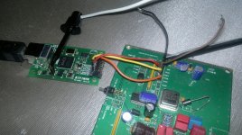
I connect XMOS to AMB y2. y2 have wm8741 + src4192 + Guido Tent XO + OPA2365 + ADP151 3.3V regulator. I remove FB1 on XMOS and use same power from DAC. This have shared ground so connect BCLK, DATA, LRCLK only. MCLK is Tent 24.576Mhz on DAC. I test with SACD rip/ PCM convert from Ray Charles, Depeche Mode, Norah Jones, Dire Straits, Berliner Philharmoniker, etc. SMPS is no problem. Sound is excellent even like the photo. I compare with CM6631 and Fox Expresso for MCLK. XMOS is sound better. 🙂
Maybe low noise regulator will be amazing sound. I can get 1.8V regulator but hard to find low noise 1.0V. Any recommendation ?
Hi,
I connect XMOS to AMB y2. y2 have wm8741 + src4192 + Guido Tent XO + OPA2365 + ADP151 3.3V regulator. I remove FB1 on XMOS and use same power from DAC. This have shared ground so connect BCLK, DATA, LRCLK only. MCLK is Tent 24.576Mhz on DAC. I test with SACD rip/ PCM convert from Ray Charles, Depeche Mode, Norah Jones, Dire Straits, Berliner Philharmoniker, etc. SMPS is no problem. Sound is excellent even like the photo. I compare with CM6631 and Fox Expresso for MCLK. XMOS is sound better. 🙂
Maybe low noise regulator will be amazing sound. I can get 1.8V regulator but hard to find low noise 1.0V. Any recommendation ?
Attachments

strange, I mentioned the dropout issue last year and you pretended like you had never experienced it with any of your modules.... you were only running 22.57/24.xx at the time as well
I didnt believe you... I suggested that you just hadnt pushed the dac hard enough, you claimed otherwise.
its a universal problem that needs to be sorted out, you are correct though, i've found that isolating from USB ground, both through USB directly and through my USB i2c connection and running higher clock speeds has helped and using fifo with higher speed XO in sync mode makes it immune
Last edited:
Hi Caad,
I did not listen for change. I don't think it can be changed from this regulator only because dc-dc converter will still make noise.
But this device is crazy. I think it have switching so it must be bad, but it is not bad. Seem like impossible to be good, but it is very good.
So maybe my change have no big result but I change because I don't like dc-dc converter in my hifi.
I will continue the changing and finally I will listen.
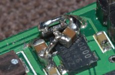
Now I change the 5V supply XMOS VSOP to 3.3V with ADP151 3.3V. I cut pcb trace, and fit ADP151 + 2uF X7R on input and output. Again, no problem, 🙂 but maybe XMOS feel a little bit hotter. I forget to measure temperature before so this is unreliable guess.
I must wait for TLV part to finish changing.
I did not listen for change. I don't think it can be changed from this regulator only because dc-dc converter will still make noise.
But this device is crazy. I think it have switching so it must be bad, but it is not bad. Seem like impossible to be good, but it is very good.
So maybe my change have no big result but I change because I don't like dc-dc converter in my hifi.
I will continue the changing and finally I will listen.
Now I change the 5V supply XMOS VSOP to 3.3V with ADP151 3.3V. I cut pcb trace, and fit ADP151 + 2uF X7R on input and output. Again, no problem, 🙂 but maybe XMOS feel a little bit hotter. I forget to measure temperature before so this is unreliable guess.
I must wait for TLV part to finish changing.
Attachments
switchmode power supplies, if designed properly can be lower noise than almost any other type, especially down in the low frequencies where it matters for audio. with everything in the right place (filtering, EMC etc) with a good design, I would take a switchmode supply over a linear one for lower budget stuff. this is one area that audiophile 'wisdom' is wrong, still stuck in the ancient past. regulation at high frequencies, like we see in digital logic is better suited for switchmode than an LDO, which usually have pretty average dynamic performance and rely on the caps for transient response.
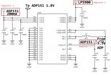
The 1V supply may need over 300mA when workingThis XMOS use ~155mA. I change 1.8V to ADP151. No problem. For 1.0V I will try TLV71210.
There is no headroom when using TLV71210 and according to the famous P=VI equation, if the LDO is 3.3V input 1V output, P=2.3V*0.3A, the small LDO need the dispatch 0.69W when running, it will be quite hot. If the input is 5V, 1.2W is converted to heat in the LDO, it should overheat immediately...
Last edited:
Thank you for this warning. Maybe this is not for other diyer to copy. 😱 And maybe no reason to copy. 😉 Although the datasheet says 10mV noise, but sound is excellent. 🙂
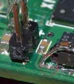
This is current working power. Device have two main 3.3V regulator and this is no problem at this time but I will test longer. 3.3V ADP supply power for 1.0V and 1.8V. XMOS is 49 deg C. Total current is 155mA. Current only change small amount for sample rate change.
I want to fit 1.0V ldo and if it is working, then remove power to VSUP (M1 M2 H1) so no switching noise. This can work if current enough ? VSUP only supply DC converter ?
Thank you !
EDIt - I also try usb isolator adum4160. It cannot work but this is not surprise. Also, maybe regulator 2 is better @500mA like LT1763, ADP7104, etc.
Attachments
Last edited:
... I also found that the I2S output timing is very tight, as the I2S data is read at the falling edge of bck according to the philips datasheet(if I don't read it wrong),
I am thinking of adding a delay in the firmware and moving the falling edge of BCK to the center of the data bit, much more headroom for the DAC(if direct connect) or reclock ...
I'm afraid that you have misunderstood the I2S standard.
http://www.classic.nxp.com/acrobat_download2/various/I2SBUS.pdf
After SD is asserted and it remains stable enough, a rising edge of SCK(BCLK) indicates the timing of latch.
All signals are of positive logic.
I'm afraid that you have misunderstood the I2S standard.
http://www.classic.nxp.com/acrobat_download2/various/I2SBUS.pdf
After SD is asserted and it remains stable enough, a rising edge of SCK(BCLK) indicates the timing of latch.
All signals are of positive logic.
somebody told there is two’s complement LSB extension error if following the datasheet when playing 16bit data to 24/32bit DAC. I will try to read it thoroughly before doing any reclock and modify the related portion of firmware if I have time😀
The 1V supply may need over 300mA when working
There is no headroom when using TLV71210 and according to the famous P=VI equation, if the LDO is 3.3V input 1V output, P=2.3V*0.3A, the small LDO need the dispatch 0.69W when running, it will be quite hot. If the input is 5V, 1.2W is converted to heat in the LDO, it should overheat immediately...
Hi,
I think NCP694 is a better regulator for this to be safe. It is 6V input max, 1A load and 30uV noise. I can add 6.8R 1W series resistor to input. This can share load from 5V for less heat and also be RC filter. Resistor rating P = I x I x R = 0.09R @300mA.
Datasheet says M1 and M2 are input for DC converter. They have a share trace so I can cut. What s H1 ? Datasheet also says DC converter can turn off in registry.
So I order parts. As I am waiting, I have listened for changes. I think XMOS is improved with low noise regulators. 🙂 I see the 48.000Mhz xo use 1.8V so I think I can understand the reason.
Last edited:
No output impedance of NCP694 is provided in the datasheet. Same for TLV71210... Their transient performance charts should be compared...
Output noise is not important as we power so crude thing as uC core - it's noise wil be MUCH higher then regulator's.
It's all about reg's output impedance, and its ability to regulate the load = suppress it's noise.
Output noise is not important as we power so crude thing as uC core - it's noise wil be MUCH higher then regulator's.
It's all about reg's output impedance, and its ability to regulate the load = suppress it's noise.
Last edited:
I understand but I cannot get information. So I guess for more current ability = lower output impedance, so NCP ( I get 694H not 694D, D have extra transistor with more RDS ) better than TLV, and it is more safe. Can you recommend a part ? I ask before but no answer.
Or maybe DC converter can keep using ?
Well, I choose NCP because this is best part I can buy, and I will use 470uF or bigger, very low esr solid polymer cap. 😀
Or maybe DC converter can keep using ?
Well, I choose NCP because this is best part I can buy, and I will use 470uF or bigger, very low esr solid polymer cap. 😀
Last edited:
For hack discussion - how many choices for ways to fit this regulator. On top side, for short trace to XMOS but low heat dissipation. On ground plane for best heat dissipation but longer trace. Any other choice ? What is the favourite way and why ? 🙂
Hi guys,
Apologies i've not had time to reply to the PM's I have received yet. Had a very busy tail end of the week, I will try and get to them today.
I noted some questions regarding layout for the U8 PSU. The current public data-sheet states:
The most important thing you can do here is getting C1 as close to the XMOS device as possible - C2 can be omitted. The example schematics in the data-sheet are to be updated very soon (I believe there is a release scheduled this week).
(Also XMOS have standardised on the use of a "V" prefix for power supply references, but some "P" prefixes seem to remain, this will be fixed in the next release)
Apologies i've not had time to reply to the PM's I have received yet. Had a very busy tail end of the week, I will try and get to them today.
I noted some questions regarding layout for the U8 PSU. The current public data-sheet states:
The DC-DC converters should have a 4.7uF X5R or X7R ceramic capacitor and a 100nF X5R or X7R ceramic capacitor on the PSUP input pins M1 and M2. These capacitors must be placed as close as possible to the those pins (within a maximum of 5mm), with the routing optimized to minimize the inductance and resistance of the traces.
The most important thing you can do here is getting C1 as close to the XMOS device as possible - C2 can be omitted. The example schematics in the data-sheet are to be updated very soon (I believe there is a release scheduled this week).
(Also XMOS have standardised on the use of a "V" prefix for power supply references, but some "P" prefixes seem to remain, this will be fixed in the next release)
Hi guys,
Apologies i've not had time to reply to the PM's I have received yet. Had a very busy tail end of the week, I will try and get to them today.
I noted some questions regarding layout for the U8 PSU. The current public data-sheet states:
The most important thing you can do here is getting C1 as close to the XMOS device as possible - C2 can be omitted. The example schematics in the data-sheet are to be updated very soon (I believe there is a release scheduled this week).
(Also XMOS have standardised on the use of a "V" prefix for power supply references, but some "P" prefixes seem to remain, this will be fixed in the next release)
V or P is not any problem. 🙂 Maybe datasheet will be better if it have mA supply rating for each pin. 😉 I only see 500mW total. Maybe I miss this info ? 😕
Can you tell me please - M1 and M2 ONLY supply DC converter ? M1 and M2 not needed if DC converter not needed ?
What is H1 needed for ? Can I cut power to this pin or must always have power ? Many many thanks for these answers. It can stop me cutting wrong traces... 😱
BTW this device is U6 because it is wrong size for U8 but I think the power layout is the same.
Thank you again ! 🙂
Last edited:
... According to the official philips I2S specification(if I don't read it wrong), 32bit I2S data require 128x BCK to play. Some DAC including the famous ES9018 will have problem playing 128x BCK I2S data. The PCB I2S output specification is listed in the related item description. ...
I can't imagine how you got such understanding from the I2S standard documents. The SCK necessary for 32 bit/channel SD is just 64x.
somebody told there is two’s complement LSB extension error if following the datasheet when playing 16bit data to 24/32bit DAC. I will try to read it thoroughly before doing any reclock and modify the related portion of firmware if I have time😀
Raymond ( his user ID is RayCTech) once claimed and requested his proprietary extension method and SDTrans and exaU2I implemented the method. However, afterward, he retracted the claim without any apologies.
As described in the I2S document, you must simply set least significant data bits to '0'. It means multiplying by 8 bit or 16 bit.
Of course, you can add an appropriate dither if you want.
I can't imagine how you got such understanding from the I2S standard documents. The SCK necessary for 32 bit/channel SD is just 64x.
I do not thoroughly read the i2s datasheet yet, but the first bit of i2s data is read after one clock cycle of BCK. If one clock cycle is waste, 64x BCK should not enough to include two 32bit data?
- Status
- Not open for further replies.
- Home
- Source & Line
- Digital Source
- New XMOS usb 384khz