glt, i won't believe there are the xtals till i see the back of the board. Somehow i have a feeling that the bottom of this board is "Solid ground plane" as advertised on eBay 🙂
The 48meg "reclock" brings even more deception...
The 48meg "reclock" brings even more deception...
Appreciate you spending time in this board.
No worries. Just taken a look at your website. Regarding your part making mystery "ES" means Engineering Sample. It's a late date code so should be final silicon.
Hello guys, hoping that I will not make any of you upset I couldn't notice the presence of XMOS employee which I want to say hello and say that I'm happy to know him by our (DIYers) side! As for discussion, I would like to stay away and keep my silence just want to add that I was/am quite concerned to add external clocks to other XMOS-based designs (no names!) 🙂 What I want to tell to glt is the fact that XMOS can easily control / be driven by external clocks in certain configuration. I work on something like this for quite some time now and attached is the result of my many nights spend in front of my LCD (when spare time was available for this pleasure). It will also support 384 Khz and based on XMOS chips (the "old" ones, without UPLI integrated in it). If my message goes in a wrong place then mods please feel free to delete it.
Kind regards,
Lorien
Kind regards,
Lorien
Attachments
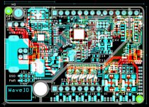
The pcb have 3 clocks. 48mhz always on ( grey xo near regulator ) for USB PHY. MCLK is from 2 Fox. The Fox turn on/off by 2 enable traces. All trace on top of board. No trace in ground plane (one small one). So it is easy to remove Fox and can use any pair of 22/24M xo.
From GLT site : http://hifiduino.wordpress.com/2013/04/16/got-the-xmos-384khz-usb-interface/
Fox

48mhz on left

LP5900 is 150mA. LP5907 is 250mA. Maybe this board need/use LP5907 because XMOS + 3 xo (1 disabled) + atmel > 150mA ? Or is XMOS use 5V and 3.3V ?
From GLT site : http://hifiduino.wordpress.com/2013/04/16/got-the-xmos-384khz-usb-interface/
Fox
48mhz on left
LP5900 is 150mA. LP5907 is 250mA. Maybe this board need/use LP5907 because XMOS + 3 xo (1 disabled) + atmel > 150mA ? Or is XMOS use 5V and 3.3V ?
Last edited:
Aha, i've clearly missed the grey oscillator and took one of the expressos for core clock and the other one - for asyncronous I2S reclocking.
This is a nice little board then, thanks for clarification!
Yet still the external oscillators input thru the connector would be great, either thru slave-compatible MCLK or by separate pins or whatever.
This is a nice little board then, thanks for clarification!
Yet still the external oscillators input thru the connector would be great, either thru slave-compatible MCLK or by separate pins or whatever.
Hello guys, hoping that I will not make any of you upset I couldn't notice the presence of XMOS employee which I want to say hello and say that I'm happy to know him by our (DIYers) side! As for discussion, I would like to stay away and keep my silence just want to add that I was/am quite concerned to add external clocks to other XMOS-based designs (no names!) 🙂 What I want to tell to glt is the fact that XMOS can easily control / be driven by external clocks in certain configuration. I work on something like this for quite some time now and attached is the result of my many nights spend in front of my LCD (when spare time was available for this pleasure). It will also support 384 Khz and based on XMOS chips (the "old" ones, without UPLI integrated in it). If my message goes in a wrong place then mods please feel free to delete it.
Kind regards,
Lorien
Hi Lorien, no problem with me. If there is a best place for "coopetition" it should be here in the diy boards 🙂. Thanks for sharing the layout. Was always curious about your next gen product. I can see the re-clocking circuitry.
No worries.
Can I ask ? It is okay to increase capacitance on DC-DC converter LC filter ? Datasheet say 22uF minimum. There is a maximum capacitance ? Maybe this can be lower noise. Thank you.
...and VSUP (M1, M2, H1) is supply only for DC-DC converter ?
I wonder if external LDO can use for VDD core (K1, K2) and disable buck converter ?
Thank you !
I wonder if external LDO can use for VDD core (K1, K2) and disable buck converter ?
Thank you !
Last edited:
Hi Lorien, no problem with me.
And for me ! Maybe do premium XMOS with 1.0V ldo, 1.8V ldo, many 3.3v ldo, cchd-957, NVE isolator, re-clock, etc ?
Thanx! I hope you do share a global opinion 🙂 Well, this new PCB had to be a surprise still I am already tired to design it over and over again (it is at the 8th big change - close to the old one). It started to be the cheapest USB to I2S interface on the planet (a subjective opinion, of course) but I guess I cannot withstand to the desire of adding few more decoupling caps or change something in stock design.Hi Lorien, no problem with me. If there is a best place for "coopetition" it should be here in the diy boards 🙂. Thanks for sharing the layout. Was always curious about your next gen product. I can see the re-clocking circuitry.
Moreover, I like to thank again to rsowen (Ross?) for his advice on metastability issues... Was not sent personally but a yellow light has lit in my head and I had to check it again to be as sure as I can that it will not happen.
As for the new XMOS chip, my personal opinion is kinda favorable: I do like the ULPI integration (this will easier lives of anyone that has to do with Microchip's inability to source own products at a proper time - me first
 ). The downside would be the integrated PSUs: for marketing purposes this is a very good thing (the result will be compact card, lower costs, easy integration and so on) BUT when it comes to audiophile "insanity" (can I call it this way?), SMPSs are a no go... at least for my own one (unless the design is highly filtered). This was the main reason for switching back to old chips and choose freely the LDO paths even if the power consuming is a little bit higher (whatever that means). As I see it lately, this will be a isolated problem only for those who choose to power up any of the USB to I2S cards from USB bus and not by using external power sources.
On another hand I must search and see if there's any chances for XMOS to improve(?) anything on the I/O ports related to external clocks and how are treated into the chip. For anyone that comes from PLD world or had to do anything with it, the resampling idea of external clock, not to mention adding SMPS circuitry into the game will be close to a dead zone, at least for me.
Cheers,
L
Last edited:
adding SMPS circuitry into the game will be close to a dead zone, at least for me.
Cheers,
L
Maybe okay in special example but datasheet says 10mV. 😱
I am
 when I see
....but maybe can sound good with changes ?
So...
... increase capacitance on DC-DC converter LC filter ?
...and VSUP (M1, M2, H1) is supply only for DC-DC converter ? Disable buck converter ?
...and external LDO can use for VDD core ?
Last edited:
LP5900 is 150mA. LP5907 is 250mA. Maybe this board need/use LP5907 because XMOS + 3 xo (1 disabled) + atmel > 150mA ? Or is XMOS use 5V and 3.3V ?
... increase capacitance on DC-DC converter LC filter ?
...and VSUP (M1, M2, H1) is supply only for DC-DC converter ? Disable buck converter ?
...and external LDO can use for VDD core ?
The very first on designing a PCB is thoroughly understand it's power requirement in every possible loading condition😀
althought the latest xmos specification of this new chip still have no detail power consumption on each voltage.
but no need to worry, there are still over 50% headroom for the LP5900 in the current pcb power arrangement.
the original XMOS require a power up sequence of different voltage, the new chip should also this requirement but the datasheet still haven't this kind of information of the new chip. I think you can follow the old xmos chip datasheet and it should work.
And for me ! Maybe do premium XMOS with 1.0V ldo, 1.8V ldo, many 3.3v ldo, cchd-957, NVE isolator, re-clock, etc ?
Disagree.
microvia resistance negligable and for decoupling is imaterial, it is inductance that is the concern (approx 0.0004 Ohms).
4 layers would allow for interplane capacitance on the power pair, improving decoupling, this would improve the decoupling further and would allow more room to optimise routing. Also it would improve the impedance of the power supply to the pins of the device and the decoupling caps.
This would also allow for a decent ground plane directly under the top layer optimising signal transmission. For the difference in cost you would get a much better product, and more in keeping with a higher end audio image.
Microvias would be a bit of overkill for this design, but personaly I would feal better parting with my money if it was a 4 layer design. Even nicer but costly would be a HDI design with outer layers all ground and signal burried on the first layer down.
All that said the simplicity of the design allows it to be done on two layers and work, the above points I made are just going the liitle bit extra for the best signal integrity.
Yes and agree! I am working on one like this config but for my personal use, the c/p ratio of this baby should be too low for most diyer to have their interest
Good luck with it I say 🙂 You mention modding, is your vision hardware mods only or software also? If the latter, I see the module has a flash on board, is this security protected at all, or are you expecting people to play with the software also?
I agree.
Most diyer like hardware mods and it's the most easy zone to squeeze everything from the module,
software mod will need a complete xmos development kit and reading all the related programming document, it's much harder.
I still have many idea with it and security protected is at lower polarity
On another hand I must search and see if there's any chances for XMOS to improve(?) anything on the I/O ports related to external clocks and how are treated into the chip. For anyone that comes from PLD world or had to do anything with it, the resampling idea of external clock, not to mention adding SMPS circuitry into the game will be close to a dead zone, at least for me.
Cheers,
L
I am very happy the pioneer of xmos i2s module is involved in this thread!
I also found that the I2S output timing is very tight, as the I2S data is read at the falling edge of bck according to the philips datasheet(if I don't read it wrong),
I am thinking of adding a delay in the firmware and moving the falling edge of BCK to the center of the data bit, much more headroom for the DAC(if direct connect) or reclock
Last edited:
Old XMOS use external 3.3V and 1.0V supply and no internal smps. Designer can choose linear reg. New XMOS must use internal smps ? I hope no. No info in old and new datasheet on this.
Maybe Mr Owen can help ?
So...
... increase capacitance on DC-DC converter LC filter ? Any limit or problem ?
...and VSUP (M1, M2, H1) is supply only for DC-DC converter ? Disable buck converter by no VSUP ? Or very clean supply ?
...and external LDO can use for VDD cores, 1.0V and 1.8V ? If yes, what pin ?
Last edited:
Old XMOS use external 3.3V and 1.0V supply and no internal smps. Designer can choose linear reg. New XMOS must use internal smps ? I hope no. No info in old and new datasheet on this.
Maybe Mr Owen can help ?
So...
... increase capacitance on DC-DC converter LC filter ? Any limit or problem ?
...and VSUP (M1, M2, H1) is supply only for DC-DC converter ? Disable buck converter by no VSUP ? Or very clean supply ?
...and external LDO can use for VDD cores, 1.0V and 1.8V ? If yes, what pin ?
the effect of increase capacitance on DC-DC converter LC filter is included in all basic theory of all DC-DC converter😀according to the datasheet, the switching frequency is 1MHz, the effect of changing capacitance and the inductance can be calculated easily.
There is only 3.3V 1.8V 1V in the new xmos, the power up sequence combination is less the 9😛 I have tried all combination in the very beginning, some work but some do not work, but I forget to write it down. Anyway it can be tested very easily, you should have fun with it.
Using external power to the 1.8V/1V is also tested in the very beginning when testing the power usage in every loading condition(different load condition includes 44.1k->384k, playing different frequency/tone in different volume, the current usage change when changing music volume, the effect of increase oscillator frequency to each voltage power usage... etc.,)
the datasheet has the pin location for 1.0V and 1.8V. You can simply remove the inductor and supply external 1v and 1.8V power to the positive pin of the 22uf capactor, be care overvoltage and reversevoltage can damage the xmos chip immediately. Some low quality power supply has power on overshoot, it's also danger.
Last edited:
I get my XMOS and connect to PC. 🙂 All good ! Connect to DAC tonight....
I have a question for the driver. Channel Map says 32 bit, output says 24 bit. It is 32 bit for ASIO (32 bit volume control etc) and output cut to 24 ?
Thank you.
I have a question for the driver. Channel Map says 32 bit, output says 24 bit. It is 32 bit for ASIO (32 bit volume control etc) and output cut to 24 ?
Thank you.
Hi DIYinHK.
Is it planned that the USB-module can support DSD in a future firmwareupgrade?
DSD support will be added if most diyer like to have it
I get my XMOS and connect to PC. 🙂 All good ! Connect to DAC tonight....
I have a question for the driver. Channel Map says 32 bit, output says 24 bit. It is 32 bit for ASIO (32 bit volume control etc) and output cut to 24 ?
Thank you.
According to the official philips I2S specification(if I don't read it wrong), 32bit I2S data require 128x BCK to play. Some DAC including the famous ES9018 will have problem playing 128x BCK I2S data. The PCB I2S output specification is listed in the related item description.
Last edited:
Hi
I am thinking of this board to replace the amanero usb to i2s board because of the dropout problem with the Buffalo 2 dac.
Is this an issue with this board or the other board listed with diyinhk wedpage?
I like to have dsd support if possible .
thanks
kp93300
I am thinking of this board to replace the amanero usb to i2s board because of the dropout problem with the Buffalo 2 dac.
Is this an issue with this board or the other board listed with diyinhk wedpage?
I like to have dsd support if possible .
thanks
kp93300
Hi
I am thinking of this board to replace the amanero usb to i2s board because of the dropout problem with the Buffalo 2 dac.
Is this an issue with this board or the other board listed with diyinhk wedpage?
I like to have dsd support if possible .
thanks
kp93300
the dropout problem of es9018 is very complex, power and ground plane arrangement, decouple cap, oscillator jitter etc are all related. The only 100% sure no dropout is using synchronize clocking😀 but at less 49/45M oscillator i2s module is needed for 192k operation and 98/90M is needed for 384k operation
I do not have the buffalo to test, but using our es9018 pcb, there is much more dropout if using usb power than external power supply. If human ear is subjective, the number of es9018 dropout is a very good non-subjective index😎
Last edited:
- Status
- Not open for further replies.
- Home
- Source & Line
- Digital Source
- New XMOS usb 384khz