implementing FE on big board would result in too much compromises with current traces
6L6 - you said 6 pairs..... I'm still counting 8+8 holes in upper and lower lines?
what I'm missing?
6L6 - you said 6 pairs..... I'm still counting 8+8 holes in upper and lower lines?
what I'm missing?
I own a first gen Nakamichi PA-5 and decided to look at the differences between the revised Stasis circuit from Nelson and the original Nak PA-5 to see how big the changes were.
So with zero (0/aleph) real life experience with these amps, I merely relay what i found someone post on the internet as follows:
Nakamichi PA 5 Amplifiers user reviews : 4.8 out of 5 - 6 reviews - audioreview.com
"
When I first took the PA-5 home I thought it airy and very nice..until I played Judy Collins and other high-pitched singers. They sounded truly bad,like early solid-state recievers. I put the amp on the test bench and found that it easily met all its specs. So what was wrong? Well,when I put square waves into the amp (a way of testing the transient and phase behavior of an amplifier)they did not come out the way they went in...this is never a good thing. Upon analysis I found that the feed-back loop was not configured to properly address the low midrange/upper bass. Attempting to find out what was up I called Nakamichi. Everyone I spoke to refused to talk to me about it...until I got to one brave tech who told me he knew what I was talking about but would be fired if he said anything!
Well,it turned out the solution was to examine a REAL Stasis amp and incorporate the componant feedback values into the PA-5. What a difference! The amp was warmer with better dynamics and the voices were now coherent. It seems that Nakamichi set the feedback values to make the amp look good on paper at the sacrifice of its real world
performance! At any rate the total cost of parts was $5.00
so I would not hesitate to buy this amp on the used market."
implementing FE on big board would result in too much compromises with current traces
6L6 - you said 6 pairs..... I'm still counting 8+8 holes in upper and lower lines?
what I'm missing?
8 + 8 only works on the 400mm deep case I think.
It doesn't work with the 300mm deep case.
I kind of think it should be made with 8 + 8, bare minimum and people buy the appropriate case for it.
that's what I said in first related post - grow a pair, or leave it
300 deep is just too much compromises, even for FW form factor
n
300 deep is just too much compromises, even for FW form factor
n
The UMS drilling pattern that 6L6 posted mentions 8 holes only for the 400mm deep heatsink.
So pico, will that fit your 4U x 500mm deep chassis as proposed?
Maybe you should post the 500mm heatsink UMS drilling details here for ZM - I assume this will be made up of 2 heatsinks per side.
So pico, will that fit your 4U x 500mm deep chassis as proposed?
Maybe you should post the 500mm heatsink UMS drilling details here for ZM - I assume this will be made up of 2 heatsinks per side.
Last edited:
Yes it will fit the 4U x 500mm ums+ heatsink no problems
The heatsink is completely UMS compatible.
The heatsink is completely UMS compatible.
Last edited:
Zen Mod just make it the way you think it should be made. In the long run people are going to prefer a properly designed output stage than one that is compromised just so it can fit a 300mm deep chassis
that's what I said in first related post - grow a pair, or leave it
300 deep is just too much compromises, even for FW form factor
n
I agree.
Build it properly or don't build it at all.
There are plenty of other projects for people to build, we don't need to compromise this one.
My thoughts as well, thanks pico.
No problem.
Common sense should reign supreme here.
To make the output PCB as universal as possible, a compromise might be an 8 device (4 deep) PCB with two cut lines to make it a 6 device PCB; that way you could have a 12 deep (24 devices total) 300mm monoblock chassis or an 8 deep 400mm stereo chassis.
Simply put, I was looking at the wrong diagram.  8pr is the big UMS.
You are absolutely correct, the output stage should be bigger than fits in a 300mm, as this will be have a very large heatsink requirement.
8pr is the big UMS.You are absolutely correct, the output stage should be bigger than fits in a 300mm, as this will be have a very large heatsink requirement.

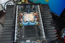
As I am one of the 2 people that Nelson graciously decided to design a new FE board for to restore the damaged Stasis amps' original FE cct brds, I thought I better jump in and publicly thank him for being so generous. Thank you Nelson! 

My only participation in the design was to give him the dimensions for the original FE boards for the Stasis II. 🙄 I haven't had any audio time recently as work has all of a sudden picked up again but I have the amp ready to rebuild this winter and the boards and parts ready to stuff. The poor Stasis has been sitting under the piano for a few years now, I am looking forward to getting it up and running again. I will be replacing all 24 output devices per side as well with new TO-3s, I think I decided on MJ21194/95 but can't recall as it's been a few years since I bought them. If you search my posts you will find my discussion with Nelson re: the repairs on this amp a few years back and my thoughts on OP devices.
Stasis II heatsink dimensions are 16" deep, 6.25" tall, 3.75" fin to mounting surface. They look like pretty standard extrusions and each side is made up of 3 pieces.
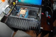
Attached pics of my baby.
Cheers
My only participation in the design was to give him the dimensions for the original FE boards for the Stasis II. 🙄 I haven't had any audio time recently as work has all of a sudden picked up again but I have the amp ready to rebuild this winter and the boards and parts ready to stuff. The poor Stasis has been sitting under the piano for a few years now, I am looking forward to getting it up and running again. I will be replacing all 24 output devices per side as well with new TO-3s, I think I decided on MJ21194/95 but can't recall as it's been a few years since I bought them. If you search my posts you will find my discussion with Nelson re: the repairs on this amp a few years back and my thoughts on OP devices.
Stasis II heatsink dimensions are 16" deep, 6.25" tall, 3.75" fin to mounting surface. They look like pretty standard extrusions and each side is made up of 3 pieces.
Attached pics of my baby.
Cheers
Attachments
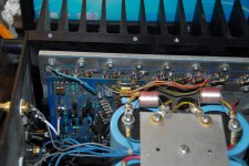
Very cool! I love those old heat sinks. Do you recall if the smaller film caps were installed from factory or were a later mod?
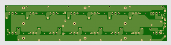
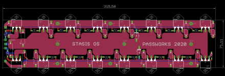
OS pcb
400 deep UMS compliant
I just need Papa to give blessing for resistor values
400 deep UMS compliant
I just need Papa to give blessing for resistor values
Attachments
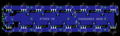

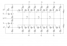
Very nice ZM, it looks bloody good, just one small point - am I missing something as I don't see the C1 and C2 on the layout. Other than that - you are a legend.
Also just looking at Nelson's new FE pcb, he has R20 and R21 already in place feeding D+ and D-, so do you also need your R1 and R2 at the input drive transistor base?
Also just looking at Nelson's new FE pcb, he has R20 and R21 already in place feeding D+ and D-, so do you also need your R1 and R2 at the input drive transistor base?
Last edited:
NICE! Are you on the payroll now?
I did that instead of Papa
though, I am sorta on payroll, all these years

Very nice ZM, it looks bloody good, just one small point - am I missing something as I don't see the C1 and C2 on the layout. Other than that - you are a legend.
Also just looking at Nelson's new FE pcb, he has R20 and R21 already in place feeding D+ and D-, so do you also need your R1 and R2 at the input drive transistor base?
caps are biggest size SMD on back side
regarding D lines resistors - I like them placed locally; considering values - you can keep both - Papas FE placed 100R, and my local 22R
- Home
- Amplifiers
- Pass Labs
- New Stasis front end