Power in W is V^2/R load
V are RMS.
50V rails will probably hit 42V maximum swing at high power because of the 1R emitter resistors.
42*.707 = 29.69
29.69^2 = 793
793/8 = 99 W
The same with 65V rails (57V swing, 40.3Vrms) gives an output of 200WPC into 8R...
Again, it is worth considering my previous admonition -
yup
thingie is able to make Klunk!, so amount of heat is strictly related to available A Class envelope, rails voltage dictating B class envelope
more pairs in OS, less critical 1R value of emiter resistor, regarding welding capability
one can make Sissy Stasis amp, with Plethora of Power, while being in danger to freeze one's butt if sitting on it, enjoying low SPL
🙂
we really need Pa to write down possible span of important resistor values in OS
ZM Knows Station, as mein Bruder Generg taught me ...... 🙂

for that , 1+5 pairs will do
rails in range of , say, 35V (even less, but sorta standard value)
.......... though - why not 1+7 pairs?
now is 5AM here, so Iq calculus is simply way above me
zzzzzzzzz Boyz, take care
rails in range of , say, 35V (even less, but sorta standard value)
.......... though - why not 1+7 pairs?
now is 5AM here, so Iq calculus is simply way above me
zzzzzzzzz Boyz, take care
Hope you had a good sleep with pleasant dreams ZM - tomorrow is another day, you stay safe and well.

as intended by Might Moi - heatsink is not pcb mounted, free mounted on puny critter, pins not fully seated in pcb
so, as I imagined, clearance there is at least 5mm
cunning plan is that builder needs to have brain engaged for most of the build
with T0220, I'm starting to worry about proper chunky size mounted and fixed heatsink at double dissipation (here less than 1W)
if thinking about my clumsiness during assembly and work, so unintentional brush on part with free mounted heatsink - lets just be more cautios
or, to avoid that - bigger pcb, care about traces beneath heatsink strictly routed at copper side etc etc
of course , when mounting fixed on pcb, some plastic spacers between sink and pcb are always cunning (again) to implement ...... had enough cases (in my service praxis) with scratched pcb stop lack, making all sorts of unexpected problems
so, when routing a pcb, I'm always taking in account worst case dumb move I can make in future; besides putting two same sex parts in complementary pair position, there are plenty of ookups I'm capable of
enclosed example of proper heatsinking of puny parts, just for giggle
Attachments

Last edited:
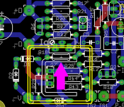
Q7-to-R18 overlap is frightening
so, it was welcome nudge
enclosed results
Attachments
Good decision, thank you. Now people can, if they so choose, use silicone adhesive to bond the heatsink to the PCB, for (a) vibration damping; and (b) better shock resistance during shipping & transport.
I wouldn't worry neither for (a) nor (b), thinking of mass of Al heatsink , sized 12square and 30 long
whichever way we do it, we are miles above, say, Musical Fidelity craftsmanship

whichever way we do it, we are miles above, say, Musical Fidelity craftsmanship
TBH though, that really is not difficult....whichever way we do it, we are miles above, say, Musical Fidelity craftsmanship

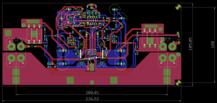
Your FE board in post #250 looks great to me ZM, I also like the idea that Mark came up with to mount it on the OS board with a couple of standoffs and very short signal connections between the 2 boards. So this FE board and the 7+1 OS board in your post #232 look like an ideal set up - has my vote for what I want to build. As a back up though I have ordered papa's FE board as well from post #1.
When and papa are happy with it all, then you can post new gerbers and away we go - but no hurry. Do you intend to test your new FE pcb design first I wonder.
When and papa are happy with it all, then you can post new gerbers and away we go - but no hurry. Do you intend to test your new FE pcb design first I wonder.
Last edited:
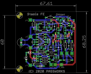
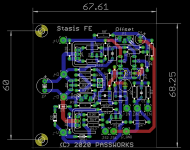
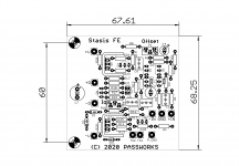
Cool Stasis FE pcb gerbers is ready available in post # 1
Thanks to the One and only Mr. PassWork
Could be possibe share pcb Stasis archive gerbers of the power output stage ready made in the past?
Thanks to the One and only Mr. PassWork
Could be possibe share pcb Stasis archive gerbers of the power output stage ready made in the past?
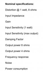
Updated DIY Stasis version post #1 nominal specyfications are ? Thanks and Kind regards 🙂
Attachments
Look at post # 1 two stages FE and OS have ready short connections..very short signal connections between the 2 boards.

But not as short as ZM's design for the FE sitting on the OS board - +D, -D, +V and -V are lined up together so will be only as long as the board spacers. Signal in and loudspeaker connections will be much the same, as will be the PSU connections.
Well if one uses say a 10mm board spacer between the 2 boards, then those connections will be 10mm long, using say a piece of tinned copper wire link. When you look at ZM,s 2 layouts the lands for those connections line up with each other. One can use what ever spacer length they like, to make sure the components mounted on the OS pcb have clearance from the FE board.
I can't see what Soundhappy is posting, but I can bet that each and every post is having nothing with technical reasons
Last edited:
- Home
- Amplifiers
- Pass Labs
- New Stasis front end