I have only just realised, following Struth's layout suggestions (post177), that the input devices are To220.
Why?
Could smaller To126 devices be used?
Could To92 devices be used?
Could sot223 devices be used?
What about a 1mm thick strip of aluminium say 15mm square with two To92 devices, or two sot223 devices, glued to each face? Gets the devices very close together and gives some extra dissipation to keep temperatures lower.
Hi Guys
I use TO-220s for the reasons outlined earlier:
The specific favoured parts are actually fully encapsulated, so there is no bare metal. This allows easy mounting with minimal hardware. The epoxy actually imposes a bit higher thermal resistance than having a single layer of mica between the tabs, but thermal tracking is "good enough" in this app.
Also, the 2SA/2SC devices specified far outperform any TO-126 I've found. For the sake of pennies, I prefer the larger case.
Personally I can't deal with soldering surface-mount components, so stick with through-hole wherever I can. SM tends to make things less easy to service for those unfamiliar with the techniques to solder the parts. Yes, there are definite advantages to the small package sizes, as was demonstrated in Suzy J's "Little Fish" amp, and as would likely benefit Lineup's circuit. However, for most hobbyists, SM is just not "friendly".
Have fun
Kevin O'Connor
So, you remember Suzy's amplifier.
She was really a good and interesting designer.
I wish was back.
She was really a good and interesting designer.
I wish was back.
Hi Guys
Yes, Suzy was great.
I downloaded her entire article to save for reference. Later I found she had pulled it down after someone commercialised her project - going so far as to use her text in their description! No acknowledgement. She was rightfully disappointed.
By the way, did I mention how many LU buffers I've sold... hehe...
Have fun
Kevin O'Connor
Hi Guys
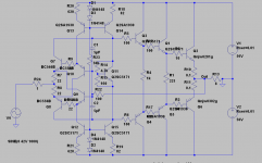
Here is a schematic and component layout for my "slow" version of the LU buffer. I call it the Diamond Feedback Buffer, or DFB.
This uses Rs instead of CSs, bootstrapped to make better use of the supply rails. Mine are just +/-12V or so and I really only need a watt or so, per channel. Biasing is class-A with the output current monitored and locked in place, as shown in a previous post.
My diamond is comprised of TO-92s, set in two flat-to-flat pairs. To improve thermal tracking, these can be linked with a piece of flat aluminum between all four devices, then heat shrinked.
J2 provides optional connection of feedback points to a voltage amplifying stage if one wants to experiment with global feedback. R33,34,35 and C9 provide alternate compensation schemes for various stand-alone and composite configurations.
The buffer performs well enough "open-loop", which is actually a misnomer here as the diamond buffer itself is a feedback loop. This really obsoletes class-i and Hawksford error-correction at least for a stand-alone buffer. My Radford LDO and THD analyser only resolves down to 0.002%, and this buffer lives below that figure across the audio band at 1W.
Q15/16 are wired as low-noise zeners across the bootstrap caps and can be eliminated without much issue. I put them in to maintain a constant voltage across the diamond BJTs for the signal range that I need.
R25 is a low-value choke, say 2-10uH.
Where distributed capacitance by way of parallel smaller values provides a better high frequency response for the supply itself, I opted for 25mm dia snap-mounts that I already have. These are 33mF-16V Panasonic TS-series. Their ripple current rating is monstrous compared to what is needed here, so they should far exceed the 3k hr rating.
Have fun
Kevin O'Connor
Attachments
Last edited:
Hi,
I made some simulation, with some other semiconductors, and with lower current ccs. It looks promising. Schematic attached.
Distortion:0.00009%, 1kHz, with 110W output, and 8ohm load. Input impedance ~10MOhm.
Sajti
Satji, great!
please show harmonics spectrum at 42Vpp
thank you in advance

Just about what I get.Spectrum attached.
Sajti
Mostly 2 and 3 and followed by slight level of Odd harmonics.
It is not what we really want,
but as the level is so low it does not really matter.
If you test the THD at 20 kHz
it is really low numbers.
Comes of that a buffer is very fast. Have large bandwidth.
Satji, great!
please show harmonics spectrum at 42Vpp
thank you in advance
I will second that 🙂, and please also try to test using a more realistic impedance (say 50 Ohm) at the input.
Thank you in advance X2
Another issue, that there is only one pair of output devices used. Doubling the number of them results much lower 5th harmonic (-138dB comparing the output level), and much less higher.
The only issue I found, that this follower needs low impedance driving. Increasing the driver impedance to 1kohm makes the distortion 10times more...
Sajti
The only issue I found, that this follower needs low impedance driving. Increasing the driver impedance to 1kohm makes the distortion 10times more...
Sajti
Just about what I get.
Mostly 2 and 3 and followed by slight level of Odd harmonics.
It is not what we really want,
but as the level is so low it does not really matter.
If you test the THD at 20 kHz
it is really low numbers.
Comes of that a buffer is very fast. Have large bandwidth.
Hi Lineup
do you think this buffer will be sensitive for back emf?
or due to gnfb which comes at high input impedance (the bases of the transistors) back emf will be damped (rather not)?
Hi,
I made some simulation, with some other semiconductors, and with lower current ccs. It looks promising. Schematic attached.
Distortion:0.00009%, 1kHz, with 110W output, and 8ohm load. Input impedance ~10MOhm.
Sajti
This one is completely unstable, try square wave test.
dado
Why not just add another diamond buffer to this scheme and turn it into a fully fledged amp with voltage gain, this would be much more usefull. As is, a voltage gain stage with low output impedance would still have to be coupled to it, lead to 2 NFB loops and added components and complexity and for what, low THD. This can be had with simpler design which could have very fast slewrate and openloop bandwith in exess of 20khz and just as low THD.
Yes it would be. But if You increase the 5pF capacitors it can be stable.This one is completely unstable, try square wave test.
dado
Sajti
Yes it would be. But if You increase the 5pF capacitors it can be stable.
Sajti
With 1 nF still not good, wrong place for a compensation.
By the way, input inpedance is much lower and changes a lot with the frequency.
dado
- Status
- Not open for further replies.
- Home
- Amplifiers
- Solid State
- New Lineup IDEA - Power Follower/Output stage