I agree emphatically with all of Bigun's points. I too have noticed that when you manage to reduce the switching issues, you find virtually no improvement in SQ. Whether there is clearly remanent crossover artefacts, OR, as Bigun suggests, the non-switching trick create other distortions, the same result - no improvement to SQ.
Feedback and careful operating points of output devices seems to fix the perceived crossover artefacts. I have found the biggest issues come from the extraction of the fb error, the voltage amplifier, and the drive stage for the output devices. These are the pre-eminent problems; solve them, and a Class AB with some global feedback sounds absolutely ethereal.
Ciao,
Hugh
Yes!

Member
Joined 2009
Paid Member
One of the big issues I have perceived with audio opinion is that there is a boat load of it based on past technology. Examples: a) electrolytic capacitors are evil - this may have been true 30 years ago when they were pretty awful but with modern materials, manufacturing etc. the quality of these beasties is soooo much better. Yes, you have to know how to use them, avoiding large a.c. voltage drops across them in the audio range (i.e. use large enough values), choosing the right cap for the job (I like bi-polar caps in the signal path). b) ceramic caps are awful so use only film caps - complete toss! Back before we had high quality multi-layer C0G/NP0 ceramics there were nasty caps out there but these C0G ceramics can outperform most low cost film caps. c) Class AB is bad - well back when we had output devices with high base currents at high collector currents (beta droop) to stress the driver stage, and high parasitic capacitances (low ft) to limit the high frequency performance maybe you could complain, but not with the superb bipolars engineered by the Japanese in the 90's, d) bass reflex speakers of old were often based on poor driver technology without the T/S based design models, modern speakers are fantastically better in these regards. And the list goes on. I feel one has to be careful to look at how old the 'advice' is and think about whether it still applies with todays materials, components and design options.
It makes sense to go further
Hi All,
Here are few thoughts, based on extensive R&D, prototyping and testing during the last year or so.
We all know the importance of a good OPS. That's the stage, operating at high currents, where any kind of distortions and artefacts are especially noticeable.
I fully agree - well-designed class AB OPS shows very good results. However - there's always some room for improvement.
First example - a very simple OPS, used in VHex+ power amp - complementary EF driver stage, follower by 2 pairs of HexFETs. Drivers are running at 12mA, output pairs - at 80-90mA each. This configuration works extremely well in relatively high loop gain design.
However, my recent simulation experiments, based on the paper on feed-forward error correction, published in 1981 by Sansui engineers (available in AES library), are showing noticeable distortion residuals reduction, especially high-frequency ones. That means - cleaner spectrums, containing less nasty crossover-related components. Live prototype is going to be tested pretty soon - we'll see the live measurements and audition test results.
The other example - NS-OPS. This one utilises dynamic bias clamping, based on the second bias spreader (voltage reference) and fast Schottky diodes, preventing the "un-used" output devices from closing. This topology has been extensively utilized by Technics in their power amps, including the very good "legendary" SE-A3, SE-A5 ones. I'm using more sophisticated CCS-ed drivers, than Technics did, allowing even more precise clamping - the drivers' base current is more constant - also reducing possible inter-modulations. This is my best OPS up till now, providing a combination of very low distortion, great stability, high speed, excellent low-ohm load driving capability (up to 595W @ 2 ohm with +/-65V rails, live tested). It sounds fantastic in any kind of design, including low-loop-gain and no-global-loop ones.
An interesting point - even with no bias clamping in place, but having the diodes, shunted by low-value capacitors, in series with the drivers' bases - the crossover components are already suppressed because of "mirrored" non-linearity, introduced by the diodes. Distortion reduction is not as high as having the clamping in place, but good enough, comparing to traditional configuration.
I don't agree with the statement that "most schematics of even high end amps don't use this at all and just go on optimizing the crossover distortion and higher loop gain". The best of them do use non-switching, error correction, differential nested feedback and other distortion reduction mechanisms in order to make the output stage as "transparent" as possible.
So, in my opinion, these distortion-reduction techniques deserve a revival.
Cheers,
Valery
Member
Joined 2009
Paid Member
So, in my opinion, these distortion-reduction techniques deserve a revival.
Cheers,
Valery
Me thinks you're the man for the job 🙂
Me thinks you're the man for the job 🙂
I'm working in a few directions
Here is some material on what is already thoroughly tested.
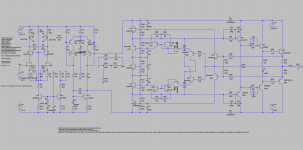
NS-OPS schematic:
NS-OPS initial design
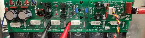
What it looks like after the great modular layout re-design, performed by Jeff:
NS Modular configuration, allowing different front-end options
Built and tested by Thimios:
NS Modular with X4 front-end - my favourite combination
Some more measurements are available down the link in my signature.
Jeff is also going to live-test the VHex+EC (the one with feed-forward EC) amplifier pretty soon - we will report on the results 😉
Cheers,
Valery
Attachments
Does Krell have something in their class A amplifier to lower the power consumption? If so, anyone have their schematic?
Hi All,
Here are few thoughts, based on extensive R&D, prototyping and testing during the last year or so.
We all know the importance of a good OPS. That's the stage, operating at high currents, where any kind of distortions and artefacts are especially noticeable.
I fully agree - well-designed class AB OPS shows very good results. However - there's always some room for improvement.
First example - a very simple OPS, used in VHex+ power amp - complementary EF driver stage, follower by 2 pairs of HexFETs. Drivers are running at 12mA, output pairs - at 80-90mA each. This configuration works extremely well in relatively high loop gain design.
However, my recent simulation experiments, based on the paper on feed-forward error correction, published in 1981 by Sansui engineers (available in AES library), are showing noticeable distortion residuals reduction, especially high-frequency ones. That means - cleaner spectrums, containing less nasty crossover-related components. Live prototype is going to be tested pretty soon - we'll see the live measurements and audition test results.
Cheers,
Valery
Can you post the circuit of these, I have no idea what you are talking about.
Thanks
Can you post the circuit of these, I have no idea what you are talking about.
Thanks
No problem - here is the original VHex+ schematic:
VHex+ schematic
Paper about the feed-forward error correction:
Design and Construction of a Feedforward Error-Correction Amplifier*
SUSUMU TAKAHASHI AND SUSUMU TANAKA
R&D Department, Sansui Electric Company Ltd., Tokyo, Japan
I don't think I can publish something of this kind here - this is a copyrighted material, although it is available free of charge for AES members.
I will also not publish the improved VHex+EC at least until we have it tested.
Cheers,
Valery
Valery:
Regarding low distortion output stages, any interest in investigating (and updating to modern times) the error correction output stage from Cordell's amp from years ago?
mlloyd1
Regarding low distortion output stages, any interest in investigating (and updating to modern times) the error correction output stage from Cordell's amp from years ago?
mlloyd1
Hi All,
Here are few thoughts, based on extensive R&D, prototyping and testing during the last year or so.
.....
Valery
Does Krell have something in their class A amplifier to lower the power consumption? If so, anyone have their schematic?
Krell engineers believe that a "tracking bias" design which continuously changed the output bias point creates audible artifacts.
Between 1992 and 2014 Krell used a Plateau Bias described in Patent Number: 5,331,291. Based upon sensed output bias voltage .AND. output transistor temperatures .AND. current driven into the speaker load, the control logic set a modestly higher than required output bias to maintain ClassA operation, up to the maximum safe limit, even for a few minutes after the transient power demands dropped. Stable, fully Class-A operation at a uniform transistor temperature and operating point for reasonable periods.
Krell's recent I-Bias tech(patent pending) adds a microprocessor plus improved analog sensors to better control "plateau bias" functions for greater accuracy and efficiency...shorter periods of necessary high Class-A bias. I-bias also provides network control which allows the owner to selectively "cap" bias current, thus allowing Class-AB operation during monster music peaks to reduce waste/heat. iBias allowed Krell to significantly reduce both physical size and fan cooling demands for HT rack mounting. YEP...fan cooled Krells that fit in HT 19" racks.
================alternative bias road==========
Study the "dual slope" Class-AB bias threads which use two opamps in the bias circuit plus ThermalTrak output transistors for very low measured distortion. A few watts of Class-A bias, plus precise ThermalTrak Vbe tracking for the output transistors creates efficient, low distortion home amps.
Andrew C. Russell uses low voltage opamps to establish a high accuracy 2-slope Vbe vs. Temp bias.
"Ideas on Temperature Compensation for Emitter Follower Triples in Class AB Audio Amplifiers"
===============
Once you add +/- 15V power supplies for an opamp DC Servo, it is easy and cheap to add a few quad comparators/opamps, plus NAND/NOR logic gates and latches from MOSFETs, for all-analog protection + Plateau Bias.
Hi
I spent some time doing simulation with LTSpice on a few circuits talked about in this thread. I simulate with only the OPS with no feedback. I just drive the voltage spreader with generator, check the biased current and plot the FFT. I cannot get good result so far. None of the case is even close to a good old simple Class AB with optimal bias.
Anyone simulated these circuit before? Can you post your .asc file? I might make wrong assumptions and don't get the good result.
Thanks
... however as a part of whole amp it works damn good!
Hi
Thanks for the info, do you have the model of all the transistors you can upload?
Thanks
they are a part of ltspice lib, I do not have separate ones...
probably if you change them to std BC550/560, BD193/140, MJE15032/33, etc, the sim will be possible!
probably if you change them to std BC550/560, BD193/140, MJE15032/33, etc, the sim will be possible!
A few thoughts.
Pawel is absolutely right - there are many nuances in the way you drive the OPS, so for the best results - simulate as close to real topology of the previous stage as possible.
Just simulate all the OPS options you compare with the same low-distortion front-end.
In my case of non-switching OPS simulation, the live prototype measurements show even better results, than simulation does. See the spectrums for NS Modular down the link in my signature. Those are the live measurements. I can hardly come close to this level of distortion for this topology in simulation 😛
I use Multisim for my simulations, so I can't show you the LTSpice model for this circuit. If Multisim one will suit you - let me know.
Cheers,
Valery
A few thoughts.
Pawel is absolutely right - there are many nuances in the way you drive the OPS, so for the best results - simulate as close to real topology of the previous stage as possible.
Just simulate all the OPS options you compare with the same low-distortion front-end.
In my case of non-switching OPS simulation, the live prototype measurements show even better results, than simulation does. See the spectrums for NS Modular down the link in my signature. Those are the live measurements. I can hardly come close to this level of distortion for this topology in simulation 😛
I use Multisim for my simulations, so I can't show you the LTSpice model for this circuit. If Multisim one will suit you - let me know.
Cheers,
Valery
Hi Valery
I drive the OPA alone only loop using voltage generator driving the top of the voltage spreader. I adjust the offset of the generator to get the output as close to 0V as possible. Then I AC couple to 2ohm load with a high value cap to run the FFT.
My idea is just looking at the distortion created only by the OPS with the bias enhancement shown in this thread. I consistently get worst distortion than when I remove the bias compensation.
I actually simulated your circuit as it really look interesting and it make sense. But I got higher distortion in the FFT when I have the bias compensation circuit in than when I just disconnect D1 and D4 in your schematic( D2 and D3 in my simulation). I play with different voltage across Q5 and Q6 (Q17 and Q18) with no luck.
What is the reason I should simulate with the whole circuit including the IPS and VAS? I worry that the feedback gain mask the distortion of the OPS alone. That's why I run OPS alone without any feedback to look at the full distortion.
Thanks
Attachments
Last edited:
they are a part of ltspice lib, I do not have separate ones...
probably if you change them to std BC550/560, BD193/140, MJE15032/33, etc, the sim will be possible!
Thanks
I'll work on it.
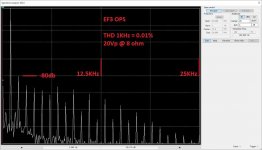
Hi Audiocrase and All,
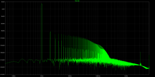
I ran some simulations, using two CCSs 5 mA each from OPS input to the rails, driving the input via 100R resistor.
At 1KHz 20Vp spectrums are rather similar.
1-st picture - traditional EF3 arrangement;
2-nd picture - NS OPS.
Simulated THD is rather close, although the one with NS OPS is a little bit higher.
I have quickly checked THD at lover output levels:
4Vp -> EF3 = 0.007% | NS OPS = 0.007%
2Vp -> EF3 = 0.003% | NS OPS = 0.003%
However, live measurements show excellent performance of NS OPS, both measured and listened.
One more thing - rather important one. NS OPS keeps low level of distortion in much wider range of the quiescent currents, which is always good to have - distortion increase when the volume goes down after running high for a long time (hot heatsinks) is a well known issue for traditional EF OPS with thermally coupled bias spreader.
Probably simulation does not reflect all the nuances of switching distortion in crossover region.
Cheers,
Valery
Attachments

Hi Valery
Thanks for your response. I am very interested in your circuit. Do you mean in your last post, you actually only simulate the OPS alone and drive the input of the OPS with 100ohm resistor and got the FFT plot?
Your result is a lot better than what I got in LTSpice simulation. It must be something I did wrong with my simulation. Can you tell me how you set the voltages on the few places I shown in my attachment? Particularly the voltage across D2 and D3. I experimented quite a bit with my simulation, the attachment show my final voltage on both the voltage spreaders. I don't know whether it is optimal or not.
Thanks
Attachments

Last edited:
- Status
- Not open for further replies.
- Home
- Amplifiers
- Solid State
- New Class A, Super-A, Non-Switching : need a revival ?