Swap power ground symbol with signal ground symbol at the bottom of C6.
Swap the signal ground symbol with the power ground symbol at both the bottom of C3 and at the input (two symbols)
The Signal Ground = Signal Return. That input circuit, both the Flow and Return halves must create a loop that starts at the source component and finishes at the source component.
The amplifier measures the voltage between the input terminals. (Signal Hot and Signal Return). The amplifier processes that information and sends a processed copy to the output terminal relative to the Power Ground. The two halves of the amplifier are doing quite different jobs. Don't mix up the currents between the two halves.
The schematic might make more sense to you, if you move the connections from the NFB and the -IN pin to actually connect with the Signal Return, i.e. all the input circuit components moved up and to the left of the chip symbol.
Physically move components R2, R3, R4, R5, C3 and C4 over to the left side of the chip.
Note that R5, R4, R3 must all connect very close to -IN PIN. Use very short traces and arrange the components so that they form a very compact shape/area.
Last edited:
Hello there
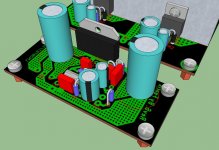
C7, C8, C9, C10 moved closer to the Chip. C7, 8 will be soldered on the track side of the PCB.
Now the mute function has both it's pads. But the Signal In only has the 'hot' In pad The Speaker has only the 'hot' Out pad and C6 has the pad to allow connection to 'signal ground'. So where do I put the 'missing' returns?
EDIT: Just caught your post Andrew. I will revisit the layout as per your recommendations.
regards
Fooboo
Attachments
Last edited:
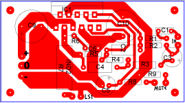
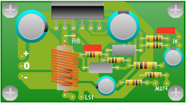
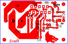
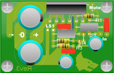
Better lay out.
Hello there
I spent this morning having another go at the PCB layout. I was aware that the traces you mentioned, Andrew, were not as short as they could be.
So I shifted the relevant components to the right of the chip and I think I have some nice short traces between the input pads and their final destination at the chip.
So here is the revised PCB pattern.
regards
Fooboo
Attachments
I don't like either of your new layouts.
I'll try again.
The powers PINs are all at the left end of the chip, PINs 1, 4 & 5. Keep the Power Input at the same end of the PCB.
The input PINs are both at the right end of the chip, PINs 9 & 10. Keep the signal input and return at the same end of the PCB. Just as importantly keep all the components that connect to the two input PINs 9 & 10 in a very small compact area. This makes them more tolerant to interference.
At post 44, bring your v- trace around the other way, which will allow your power supply interlink cable to serve as the jumper so that small signal doesn't jump over power.
Hi There
Excellent! Say it like it is 😉
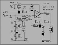
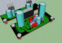
OK Here is the latest revision. I think this is more what you meant. I hope I have interpreted your guidance correctly.
R8/R9 are likely to be fitted on the track side depending on whether they can fit under the chip cleanly.
C7/C8 are not shown. They will be fitted on the track side directly to the required pins, thus -
Pin1&5 -||- Pin7 -||- Pin4
The PCB is 60mm X 37mm. Fingers crossed!
I have also attached the schematic. This is edited to reflect the advised changes.
Hi Daniel. Just saw your post. That's what I have done. Great minds etc etc
regards
Fooboo
Excellent! Say it like it is 😉
OK Here is the latest revision. I think this is more what you meant. I hope I have interpreted your guidance correctly.
R8/R9 are likely to be fitted on the track side depending on whether they can fit under the chip cleanly.
C7/C8 are not shown. They will be fitted on the track side directly to the required pins, thus -
Pin1&5 -||- Pin7 -||- Pin4
The PCB is 60mm X 37mm. Fingers crossed!
I have also attached the schematic. This is edited to reflect the advised changes.
Hi Daniel. Just saw your post. That's what I have done. Great minds etc etc
regards
Fooboo
Attachments
Earlier, I was talking about moving the trace (which you did do), but not moving the cap.
Unfortunately, now the v- cap is too far from the chip. Can you move it back to the right?
This is in regards to keeping both of the the 1500uF caps as close as possible to the chip.
Unfortunately, now the v- cap is too far from the chip. Can you move it back to the right?
This is in regards to keeping both of the the 1500uF caps as close as possible to the chip.
Last edited:
Your feedback components are way too far from the chip. Keep tracks for R3, R4, R5 as short as possible - almost up against the chip. All 'successful' designs for 3875, 3876, 3886 do this. Andrew has mentioned this a few posts ago but yours seem to be getting further and further away. Take a look at Peter Daniels designs to see how near they need to be. OK his is a minimal design without all the additional components that take up real estate and many feel are essential, but the same principle applies.
Much better.
Add power PIN decoupling. I can't see C7 & C8.
I don't like the long traces attached to PINs9 & 10 (the +IN & -IN)
Draw the input signal circuit Flow and Return. Include the DC components and the HF AC components. Now shade in the "area" enclosed within all those traces and components. That is the aerial picking up interference. Minimise Loop Area.
If it helps your layout and you don't mind having off board components, then try moving L1//R7 to the cable pair that goes to the speaker terminals. Remember Flow and Return Current Pairs applies to all circuits.
Last edited:
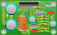
Hello there
Daniel - A compromise. I swapped C9 and C10 around. This has reduced the distance from C9+ to pin 4 and although C10 has moved further away the change in distance is minimal. Both are about the same distance.
nigelb001 - Thanks for the tip. My understanding of 'shorter' traces was based on a 'relative' scale 🙄 They are now much shorter....... I hope.
Andrew - It's getting there 🙂 Once each revision is done it does become apparent, up to a point, that things can be further tightened up. C7 is now mounted topside, I found a space, and C8 is shown in position on the trace side. Obviously when the circuit gets built C8 will be laid flat.
No problem with off board components here. R7/Inductor combo are a pain in the posterior! If I make it an off board component C9/C10 could be moved much closer to the chip. This would also allow components on the right to shunt to the left further shortening their traces.
Here is the current state of the PCB. I will try another iteration with R7/Inductor off board in the mean time. Comments welcome as always.
regards
Fooboo
Attachments
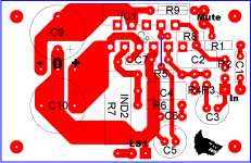
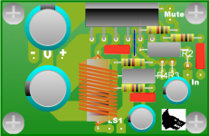
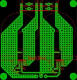
Revision 3 PCB
Hello there
Here is revision 3. R7/Inductor are now off board.
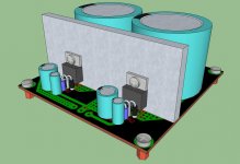
It''s a good job I checked one detail. The physical size, mainly diameter, of C9/C10. The caps from the software's built in components have the correct pin pitch but the body is 12mm diameter. The ones I can get from rapid are 16mm in diameter. You can see the silk screen outline on the component view of the 'real' components and this has guided final placement.
Lots of movement from the right to the middle of the PCB making everything more compact and shortening traces further in the important areas.
regards
Fooboo
Hello there
Here is revision 3. R7/Inductor are now off board.
It''s a good job I checked one detail. The physical size, mainly diameter, of C9/C10. The caps from the software's built in components have the correct pin pitch but the body is 12mm diameter. The ones I can get from rapid are 16mm in diameter. You can see the silk screen outline on the component view of the 'real' components and this has guided final placement.
Lots of movement from the right to the middle of the PCB making everything more compact and shortening traces further in the important areas.
regards
Fooboo
Attachments
Well, you need c9 and c10 located exactly as in post 43, but you need the V+ and V- trace routing exactly the same as post 47.
Just combine the best of both and that amplifier might play with a very nice tonality.
After seeing that possibility, I was excited. . . but I haven't seen you do it yet.
Just combine the best of both and that amplifier might play with a very nice tonality.
After seeing that possibility, I was excited. . . but I haven't seen you do it yet.
Hello there
Here is revision 4. The caps C9/C10 have been moved around again. Also the smaller components have been moved again tightening up the lay out further.
It also gave me a chance to try out Abacom's PCB design package, Sprint lay out, to draw up the revision. Not bad and being able to rotate components in as small as 5 degree increments is useful.
Also the hash filled zone may well print to a better density than a solid fill for the toner transfer.
So. What do you think of the lay out now chaps?
regards
Fooboo
PS. I think I have seen a minor change that will shorten the R3 line a tad more
Attachments
A little more tweaking. Mainly around C9/C10. 2 outlines shown which suit positioning of 19mm diameter caps down to 12.5mm diameter. Both for 7.5mm pitch but the offset allows for 5mm pitch caps to be used.
There is also a 10mm pitch which depending on the diameter of the associated cap may also be useful.
regards
Fooboo
There is also a 10mm pitch which depending on the diameter of the associated cap may also be useful.
regards
Fooboo
Attachments
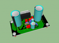
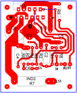
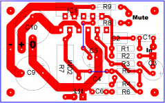
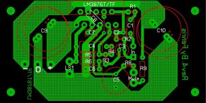
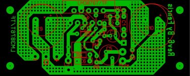
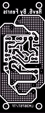
Hello there
I have managed to tighten the circuit even further
Pin 11 of the LM3876T is NC. So remove this and a small area of real estate is freed up to allow some juggling. The result is a PCB that is 30mm X 75mm. I have altered the C9/C10 cap placement to suit 5mm or 7.5mm pitch only. I have also been able to move these closer to the back edge of the PCB and therefore closer to the chip.
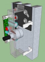
I have also changed my mind with reference to the PSU. I am going for the regulated version, as per NUUK's, site as it is significantly smaller and will fit into the proposed case much more easily.
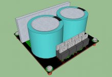
FYI. I am using Abacom Sprint-Layout for the PCB design and Google Sketchup to construct the 1:1 3D circuits. All the components are as per data sheet information which has allowed full layout testing. 😴
All I have had to do is import the exported jpg from Sprint into Sketch, as a texture, to allow correct placement of components.
regards
Fooboo.
I have managed to tighten the circuit even further
Pin 11 of the LM3876T is NC. So remove this and a small area of real estate is freed up to allow some juggling. The result is a PCB that is 30mm X 75mm. I have altered the C9/C10 cap placement to suit 5mm or 7.5mm pitch only. I have also been able to move these closer to the back edge of the PCB and therefore closer to the chip.
I have also changed my mind with reference to the PSU. I am going for the regulated version, as per NUUK's, site as it is significantly smaller and will fit into the proposed case much more easily.
FYI. I am using Abacom Sprint-Layout for the PCB design and Google Sketchup to construct the 1:1 3D circuits. All the components are as per data sheet information which has allowed full layout testing. 😴
All I have had to do is import the exported jpg from Sprint into Sketch, as a texture, to allow correct placement of components.
regards
Fooboo.
Attachments
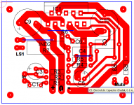
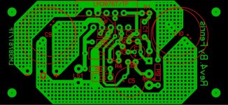
Merry Christmas all.
Further tweaking and lay out trials. I'm hoping to start ordering the components to start building my set up as soon as the festivities have passed.
I have prepped the .PDF doc which I will take to the printers and then I can then do my 'usual' toner transfer method. One change is the use of the 'groundplane' to fill the bare copper thus leaving only the minimum of copper to be etched.
regards
Fooboo
Attachments
I'm hoping to start ordering the components to start building my set up as soon as the festivities have passed.
For the capacitors that are close to heatsinks, you may want to specify the 105c models.
P.S.
Congrats on the regulated and/or capmulti power. Those options are generally higher quality. Did you up the transformer to compensate for the voltage drop?
- Status
- Not open for further replies.
- Home
- Amplifiers
- Chip Amps
- New amplifier...possibly..